Showing Spotlights 553 - 560 of 629 in category All (newest first):
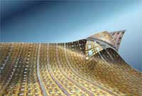
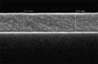 A few years ago it was discovered that the process of thermal inkjet printing can be applied to fabricate hard tissue scaffolds (such as bones) and, just recently, soft tissue with liquid biomaterials. Research is also underway to use inkjet printing for the fabrication of organic semiconductors, which, because of their low stability, will be targeted at one-time-only applications such as water purity testers. Compared to the research done with respect to organic materials, inkjet printing of inorganic materials for the formation of active devices is relatively rare. To date, only a handful of inorganic materials have been inkjet printed, primarily because of the difficulty in preparing inkjet-printable precursors. Current methods for the production of functional inorganic electronic devices are quite expensive because they require the sequential deposition, patterning, and etching of selected semiconducting, conducting, and insulating materials, involving multiple photolithography and vacuum-deposition processes. Now though, researchers have come up with a process for printable inorganic semiconductors, opening a route to the fabrication of high-performance and ultra low-cost electronics such as transparent electronics and thin film solar cells.
Mar 20th, 2007
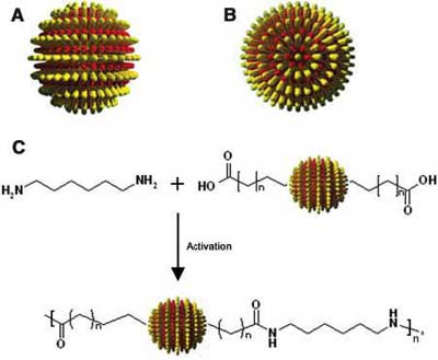
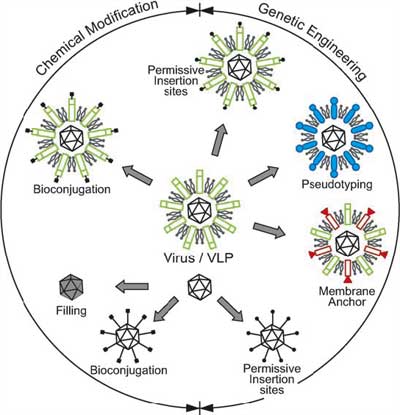 Geneticists regularly use viruses as vectors to introduce genes into cells that they are studying. Viruses are also the most common carrier vehicles in gene therapy. Having been genetically altered to carry normal human DNA, they deliver the therapeutic genes to the patient's target cells. These viruses infect cells, deposit their DNA payloads, and take over the cells' machinery to produce the desirable proteins. Current trends in nanotechnology promise to take virus technology into an entirely new direction. From the viewpoint of a materials scientist, viruses can be regarded as organic nanoparticles. Their surface carries specific tools designed to cross the barriers of their host cells. The size and shape of viruses, and the number and nature of the functional groups on their surface, is precisely defined. As such, viruses are commonly used in materials science as scaffolds for covalently linked surface modifications. The powerful techniques developed by life sciences are becoming the basis of engineering approaches towards nanomaterials, opening a wide range of applications far beyond biology and medicine.
Mar 19th, 2007
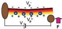 Piezoelectricity is a coupling between a material's mechanical and electrical behavior. When a piezoelectric material is squeezed, twisted, or bent, electric charges collect on its surfaces. Conversely, when a piezoelectric material is subjected to a voltage drop, it mechanically deforms. Many crystalline materials exhibit piezoelectric behavior and when such a crystal is mechanically deformed, the positive- and negative-charge centers are displaced with respect to each other. So while the overall crystal remains electrically neutral, the difference in charge center displacements results in an electric polarization within the crystal. Electric polarization resulting from mechanical deformation is perceived as piezoelectricity. This phenomenon was discovered by the brothers Pierre and Jacques Curie in 1880 and the word is derived from the Greek piezein, which means to squeeze or press. The piezoelectric effect finds useful applications such as the production and detection of sound, generation of high voltages, electronic frequency generation, microbalance, and ultra fine focusing of optical assemblies. For instance, types of piezoelectric motor include the well-known traveling-wave motor used for auto-focus in reflex cameras. A new research field, nanopiezotronics refers to generation of electrical energy at the nanometer scale via mechanical stress to the nanopiezotronic device. For example, bending of a zinc oxide nanowire transforms that mechanical energy into electrical energy. This new approach has the potential of converting biological mechanical energy, acoustic/ultrasonic vibration energy, and biofluid hydraulic energy into electricity, demonstrating a new pathway for self-powering of wireless nanodevices and nanosystems.
Mar 14th, 2007
 Since their discovery in the early 1990s, carbon nanotubes (CNTs) and carbon nanofibers (CNFs) have been used in a wide variety of applications. They have become indispensable in nanosciences and nanotechnology. However, because their production on an industrial scale remains expensive, their commercial use in such areas as catalysis has remained unthinkable. Current production processes including preparation of the support, normally silica or alumina, and impregnation with catalytically active metal for hydrocarbon decomposition, are not suitable for mass production. Researchers in Germany now report the fabrication of carbon nanotubes and carbon nanofibers on Mount Etna lavas used both as support and as catalyst, the first step for industrial production without preparation of support and its wet-chemical treatment. Such fabrication of CNTs/CNFs on naturally occurring minerals without synthetically prepared catalyst could pave the way for further exploitation of the superior properties of tailored nanostructured carbon for large-scale applications, such as catalysis and water purification by adsorption.
Mar 9th, 2007
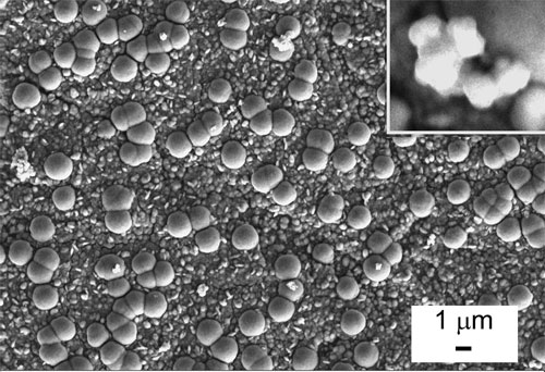
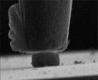 The earliest forgings, appearing around 1600 BC, were crudely hammered ornaments from naturally occurring free metals. The latest, most state-of-the-art forging techniques use micron-sized hammers to forge nanometer-sized metal shapes to be used as components in nanotechnology and microtechnology systems. New research demonstrates the possibilities of nanoforging - applying conventional metal shaping techniques to nano objects. In recent years, nanoscale fabrication has developed considerably, but the fabrication of free-standing nanosize components is still a great challenge. The ability to produce high-strength metallic components with characteristic dimensions of nanometers by nanoforging opens up new possibilities to eventually produce complex microsystems by assembling free-standing nanoscopic components. At these sizes they are of the same dimensions as micro-organisms and therefore sufficiently small even to travel through the human body.
Mar 7th, 2007
 Nanoelectronics devices often are made by integrating dissimilar classes of semiconductors and various other disparate materials into one heterogeneous single system. The two primary modes of combining these materials - mechanical bonding and epitaxial growth processes - place stringent requirements on the ultimate scale or constituent materials of circuits. With mechanical bonding, there is a limited ability to scale to large areas (i.e., larger than the wafers) or to more than a few stacking layers; incompatibility with unusual materials (such as nanostructured materials) and/or low-temperature materials and substrates; challenging fabrication and alignment for the through-wafer electrical interconnects; demanding requirements for planar bonding surfaces; and bowing and cracking that can occur from mechanical strains generated by differential thermal expansion and contraction of disparate materials. Epitaxy avoids some of these problems but places severe restrictions on the quality and type of materials that can be grown. Using a process akin to the printing press, researchers have managed to bypass the need for epitaxial growth or wafer bonding to integrate wide ranging classes of dissimilar semiconducting nanomaterials onto substrates for the purpose of constructing heterogeneous, three dimensional electronics.
Feb 27th, 2007
 While many dynamic systems are lubricated by fluids of various kinds, modern technologies, like aerospace, clean room equipment, medical devices and machines, require the application of dry coatings which exhibit reduced friction and wear. Lubrication of dynamic surfaces by fluids adds complexity, weight and cost to the system, which imposes various constraints and limits the performance of these systems. Self-lubricating coatings, i.e. coatings which exhibit reduced wear and friction without resorting to tribological fluids, have been known for many years and are in use for a variety of applications. Numerous studies have shown that different nanoparticles, impregnated into metal, polymer, ceramic and other coatings, can provide these materials with enhanced tribological performance. Prominent among these additives are the fullerene-like (IF) nanoparticles of tungsten disulfide (WS2) and molybdenum disulfide (MoS2). New research shows that it is possible to obtain self-lubrication of hard (i.e. dry) coatings such as cobalt by impregnating fullerene-like nanoparticles of WS2 in such coatings. The coating serves as a reservoir of nanoparticles which are slowly released from the surface and provide easy shear and reduced oxidation of the coating or native metal surface, which is a common phenomenon in tribology (friction and wear) of metallic surfaces.
Feb 21st, 2007
 Nanoparticles are of great scientific interest as they are effectively a bridge between bulk materials and atomic or molecular structures. Nanoparticles that consist of crystals of tens to thousands of atoms have been synthesized and used as "artificial atoms". In order to develop nanoparticle-based devices, though, it is essential to be able to control the placement of nanoparticles relative to one another. Two- and three-dimensional crystals of nanoparticles can be generated in a relatively straightforward manner, but it has been impossible to direct the assembly of the particles with any degree of specificity. The problem is that nanoparticle assembly so far has been constrained by the isotropic interactions between the particles. Isotropic materials have identical values of a property in all crystallographic directions, i.e. they are almost spherical in appearance. Though it is increasingly evident that nanoparticles would become a much more powerful research and engineering tool if it were possible to to enable directional assembly, breaking the interaction symmetry in isotropic materials is a major challenge. Doing so would enlarge the scope of potential applications, because anisotropic assemblies, where the interatomic bond strengths is directionally dependent, have distinctive properties that cannot be found or produced in isotropic assemblies. Researchers at MIT now have reported a simple method to fabricate divalent metal nanoparticles. This work is a first step towards enabling the controllable, directional assembly of nanoparticles into more complex and well-specified structures.
Feb 7th, 2007
 Subscribe to our Nanotechnology Spotlight feed