Showing Spotlights 577 - 584 of 629 in category All (newest first):
 As scientific interests and engineering applications delve down to the nanometer scale, there is a strong need to fabricate nanostructures with good regularity and controllability of their pattern, size, and shape. Furthermore, the nanostructures are useful in many applications only if they cover a relatively large sample area and the manufacturing cost is reasonable. Researchers at UCLA have now achieved a breakthrough by developing a simple but efficient fabrication method to produce well-regulated silicon nanostructures over a large sample area with excellent control of their pattern, size, and shape. Affordable surfaces with well-controlled nanostructures over a large area open new applications not only in electronics but also in the physical world through their unique properties originating from their nanoscale geometry.
Oct 27th, 2006
Adhesives may be broadly divided in two classes: structural and pressure sensitive. To form a permanent bond, structural adhesives harden via processes such as evaporation of solvent or water (white glue), reaction with radiation (dental adhesives), chemical reaction (two part epoxy), or cooling (hot melt). In contrast, pressure sensitive adhesives (PSAs) form a bond simply by the application of light pressure to attach the adhesive to the adherend. PSAs adhere instantly and firmly to nearly any surface under the application of light pressure, without covalent bonding or activation. Waterborne pressure-sensitive adhesives solve the problem of meeting environmental regulations that forbid the emission of volatile organic compounds in manufacturing. However, often waterborne PSAs have poor adhesive performance. Another problem, particularly relevant to display technologies, is how to make an electrically-conducting material that is also flexible and optically transparent. Indium tin oxide is commonly used as a transparent electrode in displays, but it is brittle and prone to mechanical failure or scratching. Adhesives can be made electrically conductive through the addition of metal particles, but then they lose optical transparency, and their adhesiveness is diminished. New research shows that waterborne PSAs containing single-wall carbon nanotubes (SWNTs) meet the requirements of environmental regulations while improving the adhesive performance. The resulting unprecedented combination of adhesion and conductivity properties holds enormous potential for demanding applications in displays and electronics.
Oct 24th, 2006
Sophisticated biomolecular motors have evolved in nature, where motor proteins actively control the delivery and assembly of materials within cells. In contrast, the development of synthetic nanomotors is in its infancy. Such nanomotors are currently explored for an increasing number of applications in hybrid bionanodevices. Along these lines, gliding motility assays, where reconstituted microtubule filaments are propelled over a substrate by surface-attached motor proteins, have been used to transport micro- and nanosized objects, such as small beads, quantum dots or DNA molecules. However, one prerequisite for controllable nanotransport is the reliable guiding of filament movement along predefined paths, a challenging task that has recently been achieved only via costly and labor-intensive topographical surface modifications. Researchers have now demonstrated a novel approach for the nanostructuring of surfaces with functional motor proteins. In contrast to all other current methods, their approach allows the three-dimensionally oriented deposition of proteins on surfaces, being the result of first binding them to the highly oriented and regulated structures of microtubules and then transferring them to the surface.
Oct 20th, 2006
Paper manufacturing is one of the mainstays of economic infrastructure and paper products influence many aspects of business and personal life. Pulping, process chemistry, paper coating, and recycling are key areas that can benefit from nanotechnology methods. One such method, layer-by-layer (LbL) assembly, is of great interest of its usage in the field of nanocoating. It allows creating nanometer-sized ultrathin films both on large surfaces and on microfibers and cores with the desired composition. Researchers at Louisiana Tech University have developed a simple and cost effective technique to fabricate an electrically conductive paper by applying layer-by-layer nanoassembly coating directly on wood microfibers during paper making process. Nanocoated wood microfibers and paper may be applied to make electronic devices, such as capacitors, inductors, and transistors fabricated on cost-effective lignocellulose pulp. The use of a conductive nanocoating on wood fibers can open the door for the future development of smart paper technology, applied as sensors, communication devices, electromagnetic shields, and paper-based displays.
Oct 18th, 2006
Controlling the shape of nanostructures is one of the challenging issues presently faced by synthetic chemists and materials engineers. Various shapes of nanomaterials, such as sphere-, rod-, wire-, triangle-, cube-, and tube-outlines have been synthesized by various approaches. However, to produce nanostructures with high monodispersity is still one of the major issues to be solved. Most work in this area focused on inorganic or synthetically organic materials. Using pure biomolecules to produce nano- or micro-structures, without the assistance of inorganic materials, is rare. Biocompatible nanospheres have been and remain of intense interest for biosensor, drug delivery, and biomedical contrast imaging. A new research report coming out of China now shows that highly monodispersed nanospheres of cystine (a sulfur-containing amino acid) aggregate were successfully produced by a quite simple method without the assistance of any other inorganic materials. This work could be of great significance in the production of nanomaterials, biosensors, and drug delivery.
Oct 17th, 2006
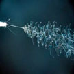 Because of the huge effective surface area, the ability to blend different types of polymers, and the fact that the process is conducted at room temperature so that biological compounds can be loaded into the fibers, electrospinning has enormous potential to create new families of higher performance products across a wide array of industry sectors. For a technique invented in 1934, we are just now beginning to see its true potential.
Oct 5th, 2006
Seashells are natural armor materials. The need for toughness arises because aquatic organisms are subject to fluctuating forces and impacts during motion or through interaction with a moving environment. Nacre (mother-of-pearl), the pearly internal layer of many mollusc shells, is the best example of a natural armor material that exhibits structural robustness, despite the brittle nature of their ceramic constituents. This material is composed of about 95% inorganic aragonite with only a few percent of organic biopolymer by volume. New research at the university of South Carolina reveals the toughening secrets in nacre: rotation and deformation of aragonite nanograins absorb energy in the deformation of nacre. The aragonite nanograins in nacre are not brittle but deformable. The new findings may lead to the development of ultra-tough nanocomposites, for instance for armor material, by realizing the rotation mechanism.
Oct 2nd, 2006
Individual carbon nanotubes (CNTs) of different structural and thus electronic characteristics can be joined to build up three-terminal logic devices. However, today this can only be achieved using highly sophisticated nanomanipulation processes. The direct growth of intrinsic functional CNT elements such as Y-shaped CNTS (YCNTs) and helical CNTs (HCNTs) can be considered as an important alternative. YCNTs already have proven to show rapid and nonlinear transistor action without the need for external gating, while HCNTs could be used as inductive elements offering rapid signal processing. Additionally, HCNTs have shown operational functionality as high sensitivity force and mass sensors and are of great interest for nanoelectromechanical systems (NEMS). A research group in Spain now reports that sulfur may be used as a highly efficient additive in chemical vapor deposition (CVD) processes, allowing enhanced selectivity in the synthesis of helical and Y-shaped CNTs.
Sep 29th, 2006
 Subscribe to our Nanotechnology Spotlight feed