Showing Spotlights 529 - 536 of 631 in category All (newest first):
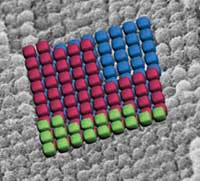 In order to exploit the unique properties of nanoscale materials for advanced applications it is often necessary to assemble nanoparticles into arrays with specific architectures. The interaction among the nanoparticles, or effects arising from their assembled larger structure, could result in interesting optical, magnetic or catalytic properties that researchers and engineers then could exploit for new materials and applications. In recent years, there has been much interest in colloidal crystals - which are examples of periodic nanoparticle arrays - as photonic crystals, templates for photonic crystals, sensors, optical and electrooptical devices, and as model systems to study crystallization processes. The success of many of these potential applications is currently limited by scientists' ability to control the structure of colloidal crystals. Normally, crystallization of uniform colloids produces face-centered cubic or hexagonal close-packing. A few other colloidal crystal structures have recently been reported, but they either require careful balance of electrostatic interactions between colloidal particles, or they rely on directing nanoparticles on a lithographic pattern that then dictates the geometry of a few layers in a thin film. New research now has resulted in a completely different and novel approach of colloidal crystallization that results in simple cubic colloidal crystals extending over many unit cells in three dimensions. Simple cubic packing is quite rare, even in atomic structures. Here, it results from combined disassembly and self-reassembly of a template- directed structure in a single reaction step.
Sep 6th, 2007
 When Gutenberg built his printing machine with moveable type in the mid 15th century, little idea did he have that he started the information age; even less that scientists would adopt the process to the nanoscale. The printing press went through several revolutionary improvements such as Lanston's monotype machine (1884), Mergenthaler's linotype machine (1886), the photo-typesetting process developed in the 1960s and finally digital printing in the 1980s. Today, printing is the most widespread technology to deposit small particles onto various surfaces. Commercial desktop laser printers use toner particles with a few microns in size while top of the line high-priced industrial printing machines sometimes already use sub-micron size particles. On the other hand, the precise positioning of nanoparticles on surfaces is key to most nanotechnology applications especially nanoelectronics. However, for automated patterning of particles, existing methods are either slow (e.g., dip-pen lithography) or require prefabricated patterns on the target substrate (e.g. for electrostatic positioning). Using a process akin to the printing press, researchers already have managed to bypass the need for epitaxial growth or wafer bonding to integrate wide ranging classes of dissimilar semiconducting nanomaterials onto substrates for the purpose of constructing heterogeneous, three dimensional electronics. Scientist in Switzerland have now developed a parallel method for the assembly and integration of a large number of bulk-synthesized nanoparticles onto an unstructured surface with high resolution and yield.
Sep 5th, 2007
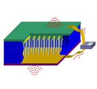
 You might have come across the acronym NBIC, which stands for Nanotechnology, Biotechnology, Information technology and new technologies based on Cognitive science. Initially introduced in the U.S. National Science Foundation's 'Converging Technologies for Improving Human Performance' report this acronym is often used to describe the basic idea that scientific and technological innovation can be stimulated through the convergence of two, three, or all four fields. At its most radical (and most controversial), proponents of convergence suggest that nanotechnologies will promote the unification of most branches of science and technology, based on the unity of nature at the nanoscale, including cognitive sciences. We'll keep you posted on this over the next few decades and see how it all works out. For the time being, though, it would be nice to be able to report on something more hands-on and - dare I write it - even practical. As it happens, scientists at the University of Toronto have done exactly that. They have demonstrated, for what appears to be the first time, the convergence of nanotechnology, microtechnology, microfluidics, photonics, signal processing, and proteomics to build a medical device that could lead to the development of fast, portable point-of-care diagnostics for infectious disease (IDs) such as HIV, SARS and many others.
Aug 31st, 2007
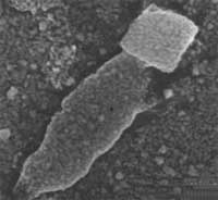 Self-assembly is Nature's way of building stuff. This fundamental principle that governs natural structures on all scales, from molecules to galaxies, generates structural organization from pre-existing parts or components. In nanotechnology, self-assembly is seen as a key technique that will one day allow the fabrication of materials and devices from the bottom up. Still only tinkering with the basics, scientists so far have designed and created simple systems that could mimic natural functions by connecting biological components to abiotic materials to understand the workings of the biological system or to take advantage of the unique properties of the nonbiological components in a natural setting. Most nanotechnologist, even if they manage to self-assemble functional nanodevices, still operate exclusively at the nanoscale (it will be a while before you can order "Tea. Earl Grey. Hot" from your food replicator in the wall). Bridging the gap between the nano- and the macroworld has proven to be a huge hurdle. In a novel approach that merges material chemistry, biology and medicine, researchers in Germany have used living bacteria to show that self-assembly of functional materials and living systems is possible through a chemically programmed construction.
Aug 16th, 2007
 An incredible amount of research has gone, and still goes, into the understanding of the properties of nanoscale particles. In order to capitalize on that research, scientists and engineers have to take the next step, which is to turn nanoparticle laboratory results into usable materials and devices. One way to use engineered nanoparticles in the real world is in thin films. Nanoparticulate thin films are thin layers, sometimes only a few nanometers thick, of composite materials that contain nanoparticles. These new materials have a wide range of applications such as nanoelectronics, magnetic storage devices, or optical coating. However, most processes used to fabricate thin nanocomposite films with high nanoparticle fillings suffer from random nanoparticle agglomeration causing formation of irregularly shaped nanostructured features within the composite. Unfortunately, the improved mechanical, tribological and electrical properties of the nanocomposites over the host matrix materials (mostly polymers) are only attainable if the nanoparticle inclusions are of uniform size and shape with very good degree of dispersion. A newly developed technique now allows a wide range of control of including metal nanoparticle into polymer matrices in a single step process.
Jul 10th, 2007
 For the over 100 million people worldwide who suffer from diabetes, testing blood glucose is the only way to be sure that it is within normal range and allows them to adjust the insulin dose if it is not. The current method for monitoring blood glucose requires poking your finger to obtain a blood sample. The equipment needed to perform the blood test includes a needle device for drawing blood, a blood glucose meter, single-use test strips, and a log book. Now imagine this scenario: your doctor implants a tiny device the size of a rice grain under your skin. This device automatically and accurately measures your blood glucose levels at whatever intervals, even constantly if required. It transmits the data to an external transceiver. If any abnormality is detected, the device warns you and automatically transmits the data to your doctor's computer. This scenario is one of the many promises of nanomedicine where in-situ, real-time and implantable biosensing, biomedical monitoring and biodetection will become an everyday fact of normal healthcare. Nanosensors are already under intense development in laboratories around the world. One of the important components for implantable nanosensors is an independent power source, either a nanobattery or a nanogenerator that harvests energy from its environment, so that the sensor can operate autonomously. Not only has such a nanogenerator now been developed, but a new prototype has been demonstrated to effectively generate electricity inside biofluid, e.g. blood. This is an important step towards self-powered nanosystems.
Jul 6th, 2007
 Continuing miniaturization has moved the semiconductor industry into the nano realm with leading chip manufacturers well on their way to CPUs using 32nm process technology (expected by 2009). There are some real challenges ahead for chip designers, particularly in moving deeper and deeper into the nanoscale, where at some point in the near future they will reach physical limits of the traditional logic MOSFET (metal-oxide-semiconductor field-effect transistor) structure. In addition to physical barriers, semiconductor companies will also reach economic barriers where profitability will be squeezed hard in view of the exorbitant costs of building the necessary manufacturing capabilities if present day technologies are extrapolated. Quantum and coherence effects, high electric fields creating avalanche dielectric breakdowns, heat dissipation problems in closely packed structures and the relevance of single atom defects are all roadblocks along the current road of miniaturization. Enter nanoelectronics (note that microelectronics, even if the gate size of the transistor is below 100 nm, is not an implementation of nanoelectronics, as no new qualitative physical property related to reduction in size are being exploited). Its goal is to process, transmit and store information by taking advantage of properties of matter that are distinctly different from macroscopic properties. Understanding nanoscale transport and being able to model and simulate nanodevices requires an entirely new generation of simulation tools and techniques.
Jul 3rd, 2007
 Nanotechnology will play an important role in future space missions. Nanosensors, dramatically improved high-performance materials, or highly efficient propulsion systems are but a few examples. In previous Nanowerk Spotlights we reported about nanotechnology propulsion technology, such as nano field emission thrusters, and the use of carbon nanotubes to harden electronic components in space. This last aspect, radiation shielding, is also where nanotechnology could make a major contribution to human space flight. NASA says that the risks of exposure to space radiation are the most significant factor limiting humans�?? ability to participate in long-duration space missions. A lot of research therefore focuses on developing countermeasures to protect astronauts from those risks. To meet the needs for radiation protection as well as other requirements such as low weight and structural stability, spacecraft designers are looking for materials that help them develop multifunctional spacecraft hulls. Advanced nanomaterials such as the newly developed, isotopically enriched boron nanotubes could pave the path to future spacecraft with nanosensor-integrated hulls that provide effective radiation shielding as well as energy storage.
Jun 29th, 2007
 Subscribe to our Nanotechnology Spotlight feed