Showing Spotlights 1713 - 1720 of 2785 in category All (newest first):
 Nanotechnology-enabled fabrication of solar cells with conventional nanoparticle-based thin-films has a drawback in that the diffusion length of the charge carriers is too short to get charge separation, although the nanoparticles themselves provide copious surface areas; whereas photovoltaic devices fabricated by aligned or partially aligned nanowire array configurations have exhibited enhanced performance owing to improved carrier collection, reduced optical reflection, and efficient absorption. While the nanowire-based approach indeed increases the diffusion length of carriers it also reduces the available surface area. However, being able to fully capture the promising surface and transport properties of nanoscale materials in practical devices or systems relies on the capability of effectively translating the extraordinary characteristics of nanoparticles or nanowires into larger-scale, three-dimensional (3D) structures. Researchers now have come up with a promising approach to address this problem by growing uniformly distributed and high density nanorods into high-aspect ratio nanochannels.
Feb 8th, 2011
 An important consideration for practical graphene applications is the fact that the physical characteristics of graphene are strongly dependent on the number of atomic planes, i.e. the properties of few-layer graphene are different from those of single layer graphene. Unfortunately, the one-atom thickness of graphene and its optical transparency make graphene identification and counting the number of atomic planes in few-layer graphene extremely challenging. This complicates the development of industrial-scale applications that would require the handling of large wafers with graphene. Current techniques for counting the number of atomic planes in few-layer graphene samples are either destructive, too complicated, or too slow. Researchers at UC Riverside have now developed a large-scale graphene recognition and quality control technique for industrial applications.
Feb 7th, 2011
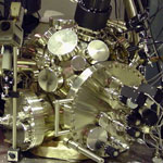
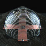 Electrically small antennas (ESA) find use in a wide variety of communications platforms - e.g. mobile phones an other handheld devices, RFID, aerospace and defense systems - but their construction requires advances in printing as well as a robust antenna design so that their operating frequency, size, and system impedance could be easily varied. Researchers have now demonstrated the conformal printing of electrically small antennas on spherical shapes with a key performance metric (radiation quality factor or Q) that very closely approaches the fundamental limit dictated by physics. This fundamental design approach enables specification of both operating frequency and size, while achieving near-optimal bandwidth at several frequencies of interest for wireless communications.
Feb 3rd, 2011
 Spinal cord injury in humans remains a devastating and incurable disorder. Rapid progress in tissue engineering, especially electrospinning techniques that lead to micro- and nanofibrous flexible tubular scaffolds for nerve cell regeneration, may lead to promising therapies for spinal cord injuries. have now demonstrated the repair of a chronically injured spinal cord by attempting to replace the fluid-filled cyst found in these lesions with a neuroprosthetics conducive to tissue reconstruction and axonal regeneration. They managed, for the first time, to obtain a consistent regeneration of the nervous tissue in chronicized injuries at the spinal cord by using a nanostructured composite scaffold with no cells in it.
Feb 2nd, 2011
 There is an increasing interest in flexible solar cells and researchers have been investigating weavable fiber solar cells based on metal wires, glass fibers, or polymer fibers. Unfortunately, the low efficiencies of these fiber-based solar cells greatly limit their promising applications. In order to improve these efficiencies, scientists are exploring various nanomaterials to improve charge separation and transport in these fiber-based photovoltaic devices. One recent promising result has been demonstrated by a research team in China who have developed a novel solar cell from flexible, light-weight, ultrastrong, and semiconductive carbon nanotube fiber. The high alignment of building nanotubes in the fiber allows charges to separate and transport along the fibers efficiently, which provides a fiber solar cell with high performance.
Feb 1st, 2011
 A caustic is the envelope of light rays reflected or refracted by a curved surface or object, or the projection of that envelope of rays on another surface. A familiar example of optical caustics is the bright line seen in a coffee cup on a bright sunny day. Here the caustic is formed by the envelope of the light rays reflected by the curved surface of the coffee cup. Caustics are formed in an anisotropic media because the direction of the group velocity and the phase velocity or the wave vector does not coincide. New theoretical work shows the existence of spin wave caustics in nanoscale ferrites, ferromagnetic and antiferromagnetic materials. Based on their theoretical results, the researchers have proposed a new device called a high frequency 'router'.
Jan 31st, 2011
 Graphene is a very interesting nanomaterial with potential for applications in many different fields including nanoelectronics. However, the properties of graphene can vary broadly and depend sensitively on its integration in device structures and the details of its interaction with other materials, such as underlying substrates or gate dielectrics. Unlike other semiconductor electronic devices, where the active layer is buried below the surface and where microscopic details of transport cannot be directly examined, graphene is exposed at a surface and can be directly examined on the atomic scale using scanning tunneling microscopy (STM) and scanning tunneling spectroscopy (STS). New work now provides microscopic details of graphene interaction with a substrate in the most common device structure used so far.
Jan 27th, 2011
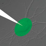 One area of nanobiotechnology that will have a massive impact on improving the live of disabled people lies at the interface (literally) between artificial functional materials and living neuronal tissues. Neuroprosthetics is an area of neuroscience that uses artificial microdevices to replace the function of impaired nervous systems or sensory organs. Different biomedical devices implanted in the central nervous system, so-called neural interfaces, already have been developed to control motor disorders or to translate willful brain processes into specific actions by the control of external devices. One are that has been quite challenging is the communication between biological tissues and artificial sensors - something that is key in building artificial retinas, for instance. Researchers in Italy have now reported the functional interfacing of an organic semiconductor with a network of cultured primary neurons.
Jan 26th, 2011
 Subscribe to our Nanotechnology Spotlight feed