Showing Spotlights 289 - 296 of 627 in category All (newest first):
 Researchers have come up with various electrode materials to improve the performance of supercapacitors, focussing mostly on porous carbon due to its high surface areas, tunable structures, good conductivities, and low cost. Graphene and carbon nanotubes show great potential but are costly. Researchers in Canada have now reported the successful hydrothermal-based synthesis of two-dimensional, yet interconnected, carbon nanosheets with superior electrochemical storage properties comparable to those of state-of-the-art graphene-based electrodes.
May 15th, 2013
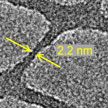
 Ferromagnetic materials exhibit the so-called anomalous Hall effect (AHE), whereby the electrons flowing through the material experience a lateral force pushing them to one side as a result of the material's intrinsic magnetization. Although the AHE has been used in the field on nanotechnology to measure the magnetic behavior of nanoparticles (with sizes larger than 50 nm), nobody so far had tried to separate the signals of the individual particles. Researchers in Germany have now developed a simple technique which allows to measure the magnetic response of single ferromagnetic nanoparticles down to a radius of about 3.3 nm.
May 14th, 2013
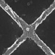
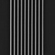
 The boundaries of electron beam lithography (EBL), the workhorse of current nanofabrication processes, is constantly being pushed further down into the single nanometer range by researchers' efforts to overcome the various limitations of EBL resolution - spot size, electron scattering, secondary-electron range, resist development, and mechanical stability of the resist. A team of scientists has now achieved the EBL fabrication of 2 nm feature size and 10 nm periodic dense structures, which are the highest resolution patterns ever achieved with common resists. The minimum feature size, 2 nm, is composed of roughly 10 atoms wide, and with just a few atoms of standard deviation.
Mar 26th, 2013
 With all the rapid progress going on in research and commercialization of flexible and transparent electronics, the obvious question is not if, but when it will be possible to build a flexible and transparent truly high performance computer. A research team has now shown, for the first time, a generic batch fabrication process to obtain mechanically flexible and transparent mono-crystalline silicon (100) from bulk wafers. The researchers demonstrate a pragmatic pathway for a truly high performance computation systems on flexible and transparent platform.
Mar 1st, 2013
 Harvesting unexploited energy in the living environment is increasingly becoming an intense research area as the global push to replace fossil fuels with clean and renewable energy sources heats up. There is an almost infinite number of mechanical energy sources all around us - basically, anything that moves can be harvested for energy. This ranges from the very large, like wave power in the oceans, to the very small like rain drops or biomechanical energy from heart beat, breathing, and blood flow. In an intriguing demonstration, researchers at Georgia Tech have now demonstrated that the technology offered by nanogenerators can also be used for large-scale energy harvesting.
Feb 28th, 2013
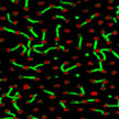 DNA is a powerful biomaterial for creating rationally designed and functionally enhanced nanostructures. Emerging DNA nanotechnology employs DNA as a programmable building material for self-assembled, nanoscale structures. Researchers have also shown that DNA nanotechnology can be integrated with traditional silicon processing. DNA nanoarchitectures positioned at substrate interfaces can offer unique advantages leading to improved surface properties relevant to biosensing (for instance, graphene and DNA can combine to create a stable and accurate biosensor), nanotechnology, materials science, and cell biology.
Feb 7th, 2013
 A key benefit of nanoimprint lithography is its sheer simplicity. There is no need for complex optics or high-energy radiation sources with a nanoimprint tool. Especially the nanopatterning of high refractive index optical films promises the development of novel photonic nanodevices such as planar waveguide circuits, nano-lasers, solar cells and antireflective coatings. Researchers have now developed a robust route for high-throughput, high-performance nanophotonics based direct imprint of high refractive index, low visible wavelength absorption materials.
Jan 29th, 2013
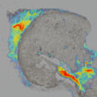 Currently, optically absorbing nanoparticles are breaking into clinical medicine because of their ability to aid in the identification of disease with several medical imaging modalities. These nanoparticles are also used in therapeutics by triggering drug release or enhancing ablation of diseased tissues, while minimizing damage to healthy tissues. The efficiency and effectiveness of the medical imaging and therapeutics using nanoparticles depends on the ability to selectively target them to the specific tissues. A novel method only uses properties of the nanoparticles and therefore are independent of the amount of nanoparticles that reaches the target location.
Jan 25th, 2013
 Subscribe to our Nanotechnology Spotlight feed