Showing Spotlights 313 - 320 of 624 in category All (newest first):
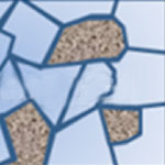 In the past couple of decades, thermoelectrics have been drawing more and more research interest due to the limited availability and the negative environmental impact of conventional energy strategies. In the past, as a measuring stick of the conversion efficiency, the term "dimensionless figure-of-merit," also referred to as ZT, has been widely used. A high ZT value usually promises high thermoelectric performance. Typically, good thermoelectric materials should simultaneously display low thermal conductivity and good electrical conductivity. Striving to enhance the performance of thermoelectric materials, researchers from Boston College and MIT have recently reported a novel materials design to achieve a 30 to 40% enhancement in the peak ZT value for n-type SiGe semiconducting alloys.
Apr 25th, 2012
 Counterfeiting of bank notes has always been a problem and central banks are leading a high-tech fight against sophisticated counterfeiting operations. For instance, when the European Central Bank designed its new banknotes, they included a variety of security features - holograms, foil stripes, special threads, microprinting, special inks and watermarks. Another high-tech approach are imprinting radio frequency identification (RFID) tags onto banknotes. While the integration of RFID technology on a banknote is technically possible, no banknotes in the world today employ such a technology. In recent work, researchers in Saudi Arabia have now fabricated the first-ever all-polymer, non-volatile, ferroelectric memory on banknotes.
Apr 23rd, 2012
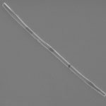 On-wire lithography is a recently developed nanotechnology fabrication technique that allows researchers to synthesize billions of gapped nanowires with nanometer control of gap length, within a single experiment. These gaps can then be used to integrate different material segments into a single nanowire in order to fabricate functional devices. In recent work, researchers have reported a simple but efficient method to use OWL to mass produce nanotube-bridged nanowires, including carbon nanotube (CNT) channels with channel lengths as small as 5 nm. Since the CNT-bridged nanowires are comprised of CNT junctions with gold electrodes, each of the nanowires could for instance work as a CNT-based sensing device, ballistic transistors, or resonators.
Apr 5th, 2012
 The concept of a 'superlens' has attracted significant research interest in the imaging and photolithography fields since the concept was proposed back in 2000. A superlens would allow you to view objects much smaller than the roughly 200 nanometers that a regular optical lens with visible light would permit. Since superlenses have demonstrated the capability of subdiffraction-limit imaging, they have been envisioned as a promising technology for potential nanophotolithography. Unfortunately, all the experimentally demonstrated photoresist patterns exhibited very low profile depths, leading to poor contrasts, which are far below industrial requirements. Researchers have now experimentally demonstrated sub-50 nm resolution nanophotolithography by using a smooth silver superlens under 365 nm UV light in a conventional photolithography setup.
Apr 3rd, 2012
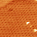 The fascination with two-dimensional (2D) materials that has started with graphene has spurred researchers to look for other 2D structures like for instance metal carbides and nitrides. One particularly interesting analogue to graphene would be 2D silicon - silicene - because it could be synthesized and processed using mature semiconductor techniques, and more easily integrated into existing electronics than graphene is currently. However, silicene does not seem to exist in nature nor is there any solid phase of silicon similar to graphite. Nevertheless, silicene has been predicted by theory as early as 1994. Researchers have now presented the first clear evidence for the synthesis and thus the existence of silicene - a two-dimensional material, with a honeycomb-like arrangement of silicon atoms.
Mar 23rd, 2012
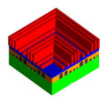
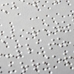 If you are a blind computer user you have to rely on electronic Braille displays which typically allow you to see only one line at a time, no matter what you were doing. Such a Braille display is a tactile, electro-mechanical device for displaying Braille characters, consisting of a row of special 'soft' cells. A soft cell has 6 or 8 pins made of metal or nylon; pins are controlled electronically to move up and down to display characters as they appear on the computer display. A number of cells are placed next to each other to form a soft or refreshable braille line. As the little pins of each cell pop up and down they form a line of braille text that can be read by touch. Researchers have now have fabricated a Braille sheet display by integrating organic thin-film transistor drivers, organic static random-access memory, and carbon nanotube-based actuators.
Mar 16th, 2012
 Polyurethane (PU) foam is an extremely versatile material that commonly is used in bedding, upholstery and building insulation. However, PU foam is very flammable, often resulting in dripping of melted material that enhances flame spread through the formation of a pool fire under the burning object. Brominated flame retardant compounds (e.g. pentabromodiphenyl ether) have been used to reduce foam flammability but there is growing evidence that these chemicals are toxic to the environment and living organisms. Replacing brominated flame retardants in polymer formulations with safer and more environmentally-friendly alternatives has also sparked the interest of nanoscientists. One recent effort to create an environmentally-friendly flame retardant system involves the layer-by-layer assembly of thin films using materials obtained from completely renewable sources.
Mar 9th, 2012
 Metal-organic frameworks (MOFs) are well-ordered, lattice-like crystals. The nodes of the lattices are metals which are connected by organic molecules. Their controlled nanometer-sized pores provide MOFs with the potential to be used in next generation gas storage, gas separation and sensors. With their special structure and large surface area, MOFs open up new opportunities for alternative systems for gas and energy storage (e.g. carbon dioxide and hydrogen storage), in catalysis, chemical sensing, as nanoreactors, and in drug delivery, making them hugely interesting for both university research and industry. Researchers have now achieved the first microfluidic method for patterning MOF crystals. As such, high-throughput single crystal patterning is achieved with an unprecedented degree of flexibility.
Feb 16th, 2012
 Subscribe to our Nanotechnology Spotlight feed