Showing Spotlights 57 - 64 of 333 in category All (newest first):
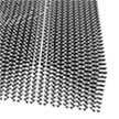 When two or more 2D materials are placed on top of each other their properties change and a material with novel hybrid properties emerges. These materials are called van der Waals heterostructures. By stacking free-standing membranes under observation in an electron microscope, researchers have demonstrated almost arbitrary 3D structures by stacking atomically thin materials, similar to a 3D printing process, where each atomic layer can be chosen from the vast library of available 2D materials.
Feb 7th, 2022
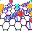
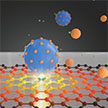 By replacing gold film with graphene, researchers have improved the performance of opto-thermoelectric tweezers. These new graphene-based opto-thermoelectric tweezers benefits from a much broader working wavelength range and a larger trapping area. They extend the working wavelength from visible band to the infrared and far-infrared bands, which are less harmful to biological samples. Owing to the ultrahigh thermal conductivity of graphene, this technology can achieve large-area particle trapping or concentration.
Jan 28th, 2022
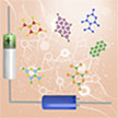
 A novel multidimensional characterization approach that combines several characterization techniques, allowing to get materials properties of the heterostructure with (almost) nanometer resolution. The method combines several microscopy tools into a multidimensional imaging tool that allows the inspection of materials' optical properties at a resolution much higher than with regular optical microscopy. At the core of this method are nanometer-resolution optical maps that we obtained with scattering Scanning Near-field Optical Microscopy (sSNOM).
Jan 22nd, 2022
 This review summarizes the current industrial graphene synthetic and analytical methods, as well as recent academic advancements in larger-scale or sustainable synthesis of graphene. Specific emphasis is placed on recent research in the use of flash Joule heating as a rapid, efficient, and scalable method to produce graphene and other 2D nanomaterials. Challenges and opportunities in the larger-scale synthesis of graphene and a perspective on the broader use of flash Joule heating for larger-scale 2D materials synthesis are discussed.
Jan 19th, 2022
 Researchers developed a holistic approach, which predicts both Li-ion storage and supercapacitive properties and hence identifies various important electrode materials that are common to both devices, may pave the way for next-generation energy storage systems. By leveraging the big-data generated by the computational pipeline, the team trains crystal graph-based machine learning models and demonstrates how this data-driven model could be helpful for the rapid discovery of potential materials from other databases.
Jan 13th, 2022
 The use of graphene-based field-effect transistors is one of the most powerful biosensing units for the detection of numerous biological and biochemical analytes. In new work, researchers propose a microscopic model of mycotoxin detection via graphene-based aptasensors enabling improvement of biosensor sensitivity, which is based on the investigation of aptamer interaction mechanism with graphene channel during binding of targeted molecules. The limit of detection is estimated at only 1 pM and time response in just 10 seconds, making the developed platform a high-performance device.
Dec 22nd, 2021
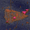
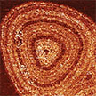 Many 2D materials with atomic-scale thicknesses suffer from oxidation and degradation effects under ambient conditions, which is one of the biggest obstacles in their practical applications. A 75-month study used atomic force microscopy to investigate the long-term evolution of oxidative defects on transition metal dichalcogenides (TMDs). Intriguingly, the researchers found that long-term storage in ambient conditions led to evolution of a distinct ring-like pattern resembling the tree-lines arising from seasonal changes.
Nov 22nd, 2021
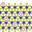
 Precise patterning of 2D materials is a route to computation and storage using 2D materials, which can deliver potentially better performance and much lower power consumption compared to the technology of today. Researchers now demonstrate an etching process that makes it possible to downsize nanostructures to the 10-20 nm range and obtain smooth edges, sharp corners, and feature sizes significantly below the resolution limit of electron beam lithography. The nanostructured 2D materials can be used themselves or as etch masks to pattern other nanomaterials.
Sep 4th, 2021
 Subscribe to our Nanotechnology Spotlight feed