Showing Spotlights 49 - 56 of 204 in category All (newest first):
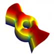 More than 25 years since the discovery of superconductivity in strontium ruthanate (SRO), understanding the properties of this material remains as challenging as ever. Researchers now demonstrated that a SRO sample can allow the two energetically degenerate condensates of Cooper-pairs with opposite momentum to segregate in domains, with a domain wall in between where chirality changes. To use the analogy to Moses parting the sea, here the Red Sea would spontaneously part into 'magenta' and 'yellow' seas on either side.
May 27th, 2020
 Those of us who work in the field of nanoscience know all about the uniqueness of the nanoscale. However, now that use cases for nanotechnology are ramping up across virtually all industry sectors, it's essential to take a step back and remember that few in the business world have experience like ours. In fact, many in the C-suite may be unsure of what nanoscience is or how their businesses could benefit from it. That's a big problem - because these decision makers are not going to support nanotechnology projects that they don't fundamentally understand. We need to rise to the challenge and start helping business leaders appreciate the distinctiveness and enormous potential of this rapidly evolving field.
May 7th, 2020
 Both display and non-display applications of liquid crystals rely on advanced liquid crystal materials. Liquid crystal materials with new functionalities can be produced by dispersing nanomaterials in liquid crystals, resulting in a mixture of nano-dopants and liquid crystals. These novel, nanotechnology-based materials very often exhibit unusual properties. For that reason, nanomaterials in liquid crystals are a hot topic of contemporary liquid crystal research and many research teams around the world carry out basic research in this field.
Mar 4th, 2020
 Oxygen reduction reaction (ORR), oxygen evolution reaction (OER), and hydrogen evolution reaction (HER) are among the core electrochemical processes in clean energy conversion and storage devices, such as metal-air batteries, water electrolyzers, and fuel cells. Single-atom catalysts have emerged as a new frontier of heterogeneous catalysts for these reactions due to their highly increased coverage of active sites, enhanced catalytic performance, and maximal metal utilization. By using machine learning algorithms, researchers provide a new paradigm for directly predicting the catalytic performance from physical properties of catalyst candidates.
Feb 13th, 2020
 Plasmonic 'nanotweezers' are structures made of noble metals that concentrate and absorb light, resulting in 'plasmonic hotspots' that make it possible to manipulate nanoscale objects suspended in a fluid. Trapping or sensing of nanoparticles using nanotweezers suffers from an intrinsic problem of low throughput as the particle delivery process is often diffusion-limited. Researhers have developed bubble- and convection-assisted trapping techniques that overcome the diffusion-limited trapping in nanoaperture tweezers and enable a reduction of 1-2 orders of magnitude in particle-trapping time compared to that of a diffusion-limited trap.
Dec 23rd, 2019
 Nanoengineering is a branch of engineering that exploits the unique properties of nanomaterials - their size and quantum effects - and the interaction between these materials, in order to design and manufacture novel structures and devices that possess entirely new functionality and capabilities, which are not obtainable by macroscale engineering. The book 'Nanoengineering: The Skills and Tools Making Technology Invisible' puts a spotlight on some of the scientists who are pushing the boundaries of technology and it gives examples of their work and how they are advancing knowledge one little step at a time.
Dec 4th, 2019
 Scientists found that size-confinement - going from macroscopic bulk samples towards nanoparticles - leads to drastic changes in the atomic structure of certain magnetocaloric materials: The change from positive thermal expansion at the macroscale towards a negative thermal expansion (NTE) at the nanoscale. NTE materials are of increasing technological interest mostly because of the idea of mixing them with a symmetric negative thermal expansion material in order to create a composite material which has near-zero thermal expansion. The nanoparticle shape is particularly suitable for the design of such composites.
Oct 10th, 2019
 2019 marks the 150th anniversary of the Periodic Table, a unique tool, enabling scientist to predict the appearance and properties of matter on the Earth and in the the Universe. Different elements have played critical roles in different periods of human activities, with silicon (Si) being a key element, at present. However, the nanotechnology age has brought different elements into the limelight and transformed their roles in science and technology. A recent article discusses the most relevant elements from a nanotechnology perspective and their applications in nanomaterials.
Oct 9th, 2019
 Subscribe to our Nanotechnology Spotlight feed