Showing Spotlights 441 - 448 of 627 in category All (newest first):
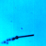
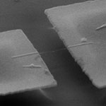 Shrinking device size to nanometer dimensions presents many fascinating opportunities such as manipulating nano objects with nanotools, measuring mass in attogram ranges, sensing forces at femtonewton scales, and inducing gigahertz motion, among other new possibilities waiting to be discovered. The two principal components common to most electromechanical systems irrespective of scale are a mechanical element and transducers. The mechanical element either deflects or vibrates in response to an applied force. Depending on their type, the mechanical elements can be used to sense static or time-varying forces. The transducers in microelectromechanical systems (MEMS) and nanoelectromechanical systems (NEMS) convert mechanical energy into electrical or optical signals and vice versa. A Spanish team has now demonstrated an ultrasensitive carbon nanotube based mass sensor in which they measured chromium atoms with a mass resolution of only 1.4 zeptograms.
Nov 18th, 2008
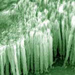 Nanostructured boron and boron-related compounds have attracted considerable scientific attention to exploit their potential use in high temperature electronics, thermoelectrics, and photovoltaics due to their unique chemical and physical properties, such as chemical inertness, hardness, and adjustable energy bandgap. Boron's theoretical tubular structures may even have higher electrical conductivity than carbon nanotubes (CNTs). So far, carbon nanotubes have been considered the most promising material for field emitters, for instance as electron emitters for field emission displays. Field emission results from the tunneling of electrons from a metal tip into vacuum, under application of a strong electric field. The small diameter and high aspect ratio of CNTs is very favorable for field emission. Due to the still existing difficulties of synthesizing CNTs with uniform chirality, a number of technical questions - such as stability, low melting point and uniformity of field emission - remain to be overcome. So scientists still looking to find other ideal candidates. New experiments conducted by scientists in China suggest that boron nanowires might fit the bill.
Oct 29th, 2008
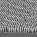 Antireflection coatings have become one of the key issues for mass production of silicon solar cells. Silicon solar cells are the most common solar cells on the market today. They are constructed with layers of n-type silicon having many electrons and p-type silicon having many electron holes. When hit by sunlight, an equal number of electrons and electron holes are generated at the interface between the two silicon layers and, as the electrons migrate from the n-type silicon to the p-type silicon, an electric flow is generated. One of the problems with silicon solar cells is the high refractive index of silicon, which causes more than 30% of incident light to be reflected back from the surface of the silicon crystals. Solar cell manufacturers have therefore developed various kinds of antireflection coatings (ARCs) to reduce the unwanted reflective losses. Currently, quarter-wavelength silicon nitride thin films deposited by plasma-enhanced chemical vapor deposition (PECVD) are the industrial standard for ARCs on crystalline silicon substrates. Unfortunately, current top-down lithographic techniques for creating subwavelength silicon gratings, such as electron-beam lithography, nanoimprint lithography, and interference lithography, require sophisticated equipment and are expensive to implement, thus contributing to the still high costs of this type of solar cells. Borrowing from Mother Nature's millions of years old design book, researchers have now come up with a nanotechnology antireflection coating inspired by the eyes of moths.
Oct 28th, 2008
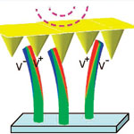 A major issue for using self-contained nanodevices, for instance as implantable nanosensors or environmental monitoring devices, is the question of how to power these tiny machines with an independent power source. Options include nanobatteries and nanogenerators that harvest energy from their environment. By converting mechanical energy from body movement, engine vibrations, or water or air flow into electricity, these nanoscale power plants could make possible a new class of self-powered medical devices, sensors and portable electronics. Probably the leading team that is driving forward the work on nanogenerators for converting mechanical energy into electricity is Zhong Lin Wang's group at Georgia Tech. Wang's team has now designed and demonstrated an innovative approach to fabricating a nanogenerator by integrating nanowires and pyramid-shaped nanobrushes into a multilayer power generator. By demonstrating an effective way for raising the output current, voltage and power, this work provides the technological platform for scaling up the performance of nanogenerators to a level that some day might be able to independently power devices like pacemakers or iPods.
Oct 27th, 2008
 Nanoscale membranes are of great interest to researchers not only for nanofiltration applications but also in areas such as flexible electronics, extremely sensitive sensors, nanomedical applications and biomolecular research. Many of these applications would require the nanomembranes to be arranged in three-dimensional structures such as tubes, helices, rings, or wrinkles. So far, the roll-up of ultra-thin layers was heavily limited in materials choice, in most cases involving epitaxial semiconductor layers. The fabrication often requires a selective underetching procedure to release the nanomembranes from their substrate, a process which not only removes the underlying sacrificial layer but also in many cases dissolves the nanomembrane material itself. A new approach developed by scientists in Germany and Hong Kong now allows controlled fabrication of pure metal and oxide tubes as well as many other material combinations. They describe a general method to produce well-defined micro- and nanotubes from thin solid films deposited by mass production tools.
Oct 21st, 2008
 The long-term vision of revolutionary bottom-up nanotechnology is based on two different concepts of molecular assembly technologies. One follows Nature's blueprint, which uses molecular recognition for self-assembly of nanoscale materials and structures; the other is man-made and uses instruments to assemble nanoscale building blocs into larger structures and devices. In contrast, the most common nanoscale fabrication techniques used today, for instance in the sub 100-nanometer semiconductor industry, are top-down approaches where fabrication technologies such as lithography or stamping are used. Here, you create ever smaller structures by starting with a block of material and remove the bits and pieces you don't want until you get the shape and size you do want. While top-down techniques can be highly parallel (semiconductor industry) it is not feasible to control single molecules with them. Using a hybrid approach that combines the precision of an atomic force microscope with the selectivity of DNA interactions, researchers in Germany have successfully demonstrated a technique that fills the gap between top-down and bottom-up since it allows for the control of single molecules with the precision of atomic force microscopy and combines it with the selectivity of self-assembly.
Oct 10th, 2008
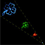
 Our Spotlight today again shows an example of the very fundamental research that is taking place in labs around the world to lay the foundation for future nanotechnology based devices. It illustrates the very early stage of development and the nature of the fundamental challenges that make up today's 'nanotechnology research. The vision of revolutionary bottom-up nanotechnology is based on a concept of molecular assembly technologies where nanoscale materials and structures self-assemble to microscale structures and finally to macroscopic devices and products. Researchers are a long, long way from realizing this vision but they are busily laying the foundation for nanoscale engineering. Assembling nanoscopic components into macroscopic materials is an appealing goal but one of the enormous difficulties lies in bridging approximately six orders of magnitude that separate the nanoscale from the macroscopic world. Right now, nanotechnology researchers have their hands full just learning how to control a straight chain of nanoparticles.
Oct 1st, 2008
 Using nanoparticles to combat cancer and a host of other diseases is an active area of research for many scientists. For decades, treating cancer has mostly involved injecting patients with toxic drugs. A practice, in which only a fraction of the drugs reach the intended target, killing healthy cells in the process and causing harmful side effects. Previous studies have shown that drug-carrying nanoparticles can accumulate in and attack tumors, in part because of their extremely small size, which helps allow them to pass through cell membranes. However, up until now, existing techniques have meant that targeting agents could only be delivered using spherical or granular shaped particles. Now, a team of scientists have demonstrated that nanoparticles designed with a specific shape, size and surface chemistry are taken up into cells and behave differently within cells depending on the characteristics of the particle.
Sep 11th, 2008
 Subscribe to our Nanotechnology Spotlight feed