Showing Spotlights 201 - 208 of 253 in category All (newest first):
 The performance of devices like organic light emitting diodes (OLEDs), flexible solar cells, or plastic electronics is sensitive to moisture because water and oxygen molecules seep past the protective plastic layer over time and degrade the organic materials which form the core of these products. To protect these sensitive devices, barrier technologies have been developed that protect them from environmental degradation. State-of-the-art barrier materials employ metal oxide thin films, commonly from aluminum or silicon oxides, which provide excellent protection from atmospheric oxygen and water, but still suffer from problems. A new study demonstrates a nanocomposite material that can initiate self-healing upon the influx of water through pores and cracks by delivering titanium dioxide nanoparticles to the defective site, which ultimately slows the rate of moisture diffusion to the reactive electronic device.
Dec 9th, 2008
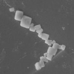
 Nanostructured boron and boron-related compounds have attracted considerable scientific attention to exploit their potential use in high temperature electronics, thermoelectrics, and photovoltaics due to their unique chemical and physical properties, such as chemical inertness, hardness, and adjustable energy bandgap. Boron's theoretical tubular structures may even have higher electrical conductivity than carbon nanotubes (CNTs). So far, carbon nanotubes have been considered the most promising material for field emitters, for instance as electron emitters for field emission displays. Field emission results from the tunneling of electrons from a metal tip into vacuum, under application of a strong electric field. The small diameter and high aspect ratio of CNTs is very favorable for field emission. Due to the still existing difficulties of synthesizing CNTs with uniform chirality, a number of technical questions - such as stability, low melting point and uniformity of field emission - remain to be overcome. So scientists still looking to find other ideal candidates. New experiments conducted by scientists in China suggest that boron nanowires might fit the bill.
Oct 29th, 2008
 Ink-jet printing of metal nanoparticles for conductive metal patterns has attracted great interest as an alternative to expensive fabrication techniques like vapor deposition. The bulk of the research in this area focuses on printing metal nanoparticle suspensions for metallization. For example, silver and gold nanoparticle suspensions have been inkjet printed to build active microelectromechanical systems (MEMS), flexible conductors and radio frequency identification (RFID) tags. Nobel metals like silver and gold are preferred nanoparticles for ink-jet formulations because they are good electrical conductors and they do not cause oxidation problems. However, gold and silver still are too expensive for most high volume, ultra low-cost applications such as RFID tags with required unit costs below one cent. A new technique developed in Switzerland uses flame spray synthesis in combination with a simple in-situ functionalization step to synthesize graphene coated copper nanoparticles which are air-stable and can be easily handled at ambient conditions. This work illustrates graphene's potential as a protective shell material for nanoparticles, enabling control and design of the chemical reactivity of non-noble metals.
Oct 14th, 2008
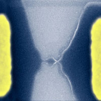
 Using single molecules as electronic components is the ultimate goal for future electronic nanotechnology devices. In order to explore the electronic properties of a single molecule, researchers have to make electrical contact between electrodes and molecules - and this has proven to be a big challenge. The problem is forming stable and reproducible molecular bridges and determining their electrical properties. It has already been shown that molecular bridges can be formed. However, their mechanical stability and reproducibility is usually low. Whether it is really possible to form a single stable molecular bridge, which can act as a 'normal' electrical component at room temperature has yet to be answered. An important step in this direction will be to identify all the mechanics involved in single atom contacts.
Oct 13th, 2008
 In contrast to the often depicted model of a perfect hexagonal lattice cylinder shape of carbon nanotubes, these nanomaterials often become twisted, bent or otherwise deformed during their growth, processing, or characterization. Researchers have found that some of these defects can be associated with a rearrangement of atoms and bonds which in turn will impact on the band structure and therefore affects the electronic properties of the tube. Previous experimental Atomic Force Microscopy and Transmission Electron Microscopy studies of carbon nanotubes have clearly identified their susceptibility to collapse and theoretical predictions of the impact that these deformations have on the electronic properties have been formulated. Experiments at the University of Surrey in the UK are the first to show atomically resolved radially collapsed double-walled carbon nanotubes, bringing also clear evidence of changes in the fundamental electronic behavior of these systems in response to the deformation.
Oct 9th, 2008
 The success of the semiconductor industry has been due in large part to its ability to continuously increase the complexity, and therefore the processing power, of integrated circuits at a given manufacturing cost. Moore?s Law observes that the number of transistors in a computer chip doubles every two years, whilst the cost of making the chip remains the same, due to miniaturization of the components. In order to produce the next generation of computer chips it is necessary to continue to shrink the size of the components on the chip. The miniaturization upon which Moore?s Law rests has been achieved through advances in the photolithographic process used to pattern the components onto to the silicon wafer. A beam of light is projected through a shadow-casting reticule and the light pattern is then directed onto a silicon wafer coated with a photochemically sensitive material, known as a resist. The solubility of the resist is modified by exposure to the light, allowing specific areas of the resist film to be removed, whilst other areas remain as a mask, so that the silicon wafer can be selectively etched, metallized or doped. For many years it has been predicted that the end of photolithography is approaching, and that further miniaturization will require next generation lithography techniques, such as EUV lithography. However, photolithography has proved remarkably resilient, and continues to improve. Unfortunately, whilst the ability of photolithography to pattern small features continues to improve, the industry is beginning to challenge the capabilities of the photosensitive resist.
Aug 5th, 2008
 We have written about scientists' fascination with graphene - the flat one-atom thick sheet of carbon - before. Over the past couple of years, graphene has become a new model system for condensed-matter physics - the branch of physics that deals with the physical properties of solid materials - because it enables table-top experimental tests of quantum relativistic phenomena, some of which are unobservable in high-energy physics. The behavior of electrons in graphene is very different from their behavior in typical semiconductors. In the latter, they possess a mass, and a finite energy (called the energy gap) is necessary to move the electrons from the valence to the conductance band and they move like regular particles, increasing their speed as they get accelerated. In graphene, electrons move with a constant speed - much faster than electrons in other semiconductors - independent of their kinetic energy (similar to the behavior of photons), and there is no energy gap. Graphene, which basically is an unrolled, planar form of a carbon nanotube therefore has become an extremely interesting candidate material for nanoscale electronics. Researchers in the UK have now, for the first time, shown that it is possible to carve out nanoscale transistors from a single graphene crystal.
Apr 23rd, 2008
 The most common type of modern transistor, and the type of transistor used in integrated circuits, is called a field-effect transistor (FET). The FET is so named because it relies on an electric field to control the shape and hence the conductivity of a 'channel' (the charge carrier) in a semiconductor material. This field causes a second electrical current to flow across the semiconductor, identical to the first weak signal, but stronger. Since the invention of the first transistor in 1947, the vast majority of electronic devices have been based on inorganic semiconductors, which in most cases has been silicon. Due to the demand for lightweight, flexible opto-electronic devices such as displays, solar cells and lasers, organic materials have become an important new class of semiconductor as they combine the virtues of plastics, which can be easily shaped, with those of semiconductors which are the basis of all microelectronics. Organic field-effect transistors (OFETs) have been mainly based on two types of semiconductors: conjugated polymers and small conjugated molecules. A recent review, published in Chemical Society Reviews, provides a general introduction about the current standing in the area of OFETs focusing on the new processable small molecules that have been recently reported for their use as organic semiconductors.
Apr 2nd, 2008
 Subscribe to our Nanotechnology Spotlight feed