Showing Spotlights 57 - 64 of 65 in category All (newest first):
 Strong and highly directional hydrogen-bonding networks are of fundamental importance in nature. Their efficiency in assisting electron-transfer processes makes them increasingly appealing for technological application inspired by biomimetic principles, i.e. the application of methods and systems found in nature to the study and design of engineering systems and modern technology. Attempting to move from microelectronics to nanoelectronics, engineers are faced with the growing difficulty of manufacturing ever tinier devices with top-down engineering approaches. They are therefore looking at possible ways for bottom-up engineering approaches with the goal of achieving the holy grail of nanotechnology - molecular self-assembly. For some time now researchers have been able to design molecules in such a way that they attach themselves to each other in alternating order, and under certain circumstances - for example on surfaces - create chains. Unfortunately the chains are not very long, because all surfaces, even extremely smooth ones, show unevenness at the atomic level. Step edges, although only a few atomic layers high, represent insurmountable hurdles to the self-assembly process, and since they are distributed randomly over the surface, the molecules form themselves into very irregular patterns. Overcoming this problem, researchers were recently able to formulate two organic molecules in such a way that they organized themselves spontaneously into long parallel chains (nanowires) on a specially prepared gold surface. Selective self-assembly on surfaces and the fundamental processes which control this phenomenon are, however, not only critical in the area of molecular electronics but also in heterogeneous catalysis - a process used in automotive catalytic converters - and in sensor technologies.
Feb 23rd, 2007
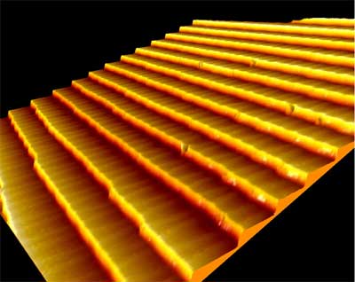
 Nanowires are expected to play an important role in the emerging fields of nanoelectronics and nanooptics. In particular, the permanently growing complexity of integrated circuit designs requires a further reduction of the size of IC components that nanowires could facilitate. Nanowires are also a possible candidate for future functional nanostructures in plasmonic devices, i.e. for information (light) propagation and manipulation below the optical diffraction limit. For these purposes, cobalt disilicide (CoSi2) is a very promising contact material due to its extremely useful properties such as low resistance, its metallic behavior, its low lattice mismatch to Si of only -1.2%. the plasmon wavelength of 1.2 micrometer, and its compatibility with modern silicon technology. Many efforts have been made to fabricate silicide nanowires employing the bottom-up approach without elaborate microlithography. Researchers in Germany now have demonstrated a promising technique that allows the defect-induced formation and placing of cobalt disilicide nanowires by focused ion beam synthesis in silicon directly where it is needed.
Jan 22nd, 2007
Bacteria are ubiquitous in the earth's surface, subsurface, fresh water, and oceanic environment. Bacteria are remarkable in that they are capable of respiring aerobically and anaerobically using a variety of compounds, including metals, as terminal electron acceptors. Metal reducing bacteria can significantly affect the geochemistry of aquatic sediments, submerged soils, and the terrestrial subsurface. Microbial dissimilatory reduction of metals is a globally important biogeochemical process driving the cycling of iron and manganese, associated trace metals, and organic matte. Microbial metal reduction is of significant interest among scientists who are researching remediation of environmental contaminants. However, little is known about the biochemical or molecular mechanisms underlying bacterial metal reduction. Conducting research with toxic metal reducing bacteria, researchers discovered that bacteria produce electrically conductive nanowires in response to electron-acceptor limitation. These findings could be used to bioengineer electrical devices such as microbial fuel cells.
Jan 3rd, 2007
'Carrier mobility' is a major factor in determining the speed of electronic devices. Aggressive scaling of the complementary metal-oxide-semiconductor (CMOS) transistor technology requires a high drive current, which depends on the charge carrier mobility. As the dimensions of nanoelectronic circuits continue to shrink, it is important that the carrier mobility does not deteriorate and, if possible, improves. The search for nanostructures where the carrier mobility values can be preserved or even improved continues owing to the extremely high technological pay-off if successful. Nanowires represent a convenient system to understand the effects of low dimensionality on the carrier drift mobility. One can also look at nanowires as an ultimately scaled transistor channel. New research at the University of California - Riverside demonstrates a method for the significant enhancement of the carrier mobility in silicon nanowires. Such mobility enhancement would allow to make smaller and faster transistors and improve heat removal.
Oct 26th, 2006
One major challenge in much of nanotechnology is how to connect nanocomponents together. Despite significant advancements in nanowire growth techniques, establishment of electrical contacts to nanowire assemblies through non-destructive methods has not yet been successfully realized. Researchers now report a novel approach toward connecting and electrically contacting vertically aligned nanowire arrays using conductive nanoparticles.
Jul 26th, 2006
Carbon nanotubes have been used as nanoreactors in a simple thermal reaction process for the fabrication of high-quality, large-yield single-crystalline magnesium nitride nanowires. These nanowires are homogeneously sheathed over the entire lengths with very thin graphitic carbon tubular layers, which effectively prevent the decomposition in the presence of water in the atmosphere.
Jun 28th, 2006
One-dimensional nanostructures such as nanowires, in particular semiconductor nanowires, have unique applications in the fabrication of nanoscale devices. How to control the growth of semiconductor nanowires is one of the most challenging issues presently faced by synthesis chemists.
Jun 23rd, 2006
 Fabrication of nanowires arrays with different patterns and separations is a major concern of the nanowire community. For this purpose, a catalyst template, which is usually a metal nanoparticle array, is needed to guide the nanowire growth.
Apr 17th, 2006
 Subscribe to our Nanotechnology Spotlight feed