Showing Spotlights 49 - 56 of 65 in category All (newest first):
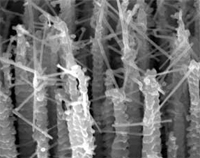
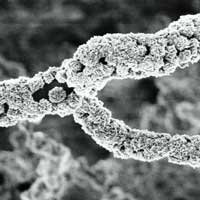 Diamonds have been known in India for at least 3000 years and are thought to have been first recognized and mined there. The most familiar usage of diamonds today is as gemstones in jewelry but, apart from being a girl's best friend, it seems that diamonds, especially nanodiamonds, are quickly becoming a scientist's best friend as well. Diamonds are the hardest natural material - the word diamond comes from the Greek term adamas, which means 'invincible' - has the lowest coefficient of thermal conductivity, is electrically insulating, chemically inert, and optically transparent. In nanoparticulate form, diamonds possess an additional property that makes them so interesting for researchers: since they are carbon-based and non-toxic they are a suitable material for drug delivery, drug diagnostics and medical imaging applications. One of the challenges in fabricating nanodiamond coatings and composite materials is the difficulty of controlling the size, texture, and crystalline quality of the diamond particles. Now, researchers in Portugal have demonstrated for the first time the facile fabrication and the conformal coating of nanocrystalline diamond onto silica nanofibers by a two-step method: synthesis of templates on silicon wafer; and coating of the silica fibers with nanocrystalline diamond.
Apr 8th, 2008
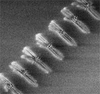
 The vision of revolutionary bottom-up nanotechnology is based on a concept of molecular assembly technologies where nanoscale materials and structures self-assemble to microscale structures and finally to macroscopic devices and products. We are a long way from realizing this vision but researchers are busily laying the foundation for nanoscale engineering. Assembling nanoscopic components into macroscopic materials is an appealing goal but one of the enormous difficulties lies in bridging approximately six orders of magnitude that separate the nanoscale from the macroscopic world. Until machinery capable of automated and industrial-scale nano-assembly can be built, the parallelism of chemical synthesis and self-assembly is necessary when controlling materials at the nanoscale. An obvious direct approach to molecular nanotechnology therefore is to start with organic molecules as building blocks. Modest from the viewpoint of molecular manufacturing visionaries, but quite fascinating to a lot of scientists, research into nanofibers, as a modification of organic crystals, is making good progress. New research results coming out of Denmark offer the basis for a novel organic-molecule-based nanotechnological concept that allows for a multitude of applications in fundamental research and in device applications. Essentially, this concept is based on three steps: 1) directed self-assembled surface growth of nanofibers from functionalized molecules; 2) transfer and manipulation of individual fibers as well as of ordered arrays; and 3) device integration.
Feb 1st, 2008
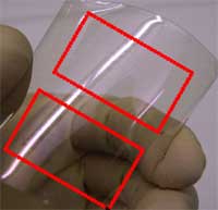
 'Smart' is the key buzz word used by materials engineers when they describe the future of coatings, textiles, building structures, vehicles and just any material that you can think of. Materials are made 'smart' when they are engineered to have properties that change in a controlled manner under the influence of external stimuli such as mechanical stress, temperature, humidity, electric charge, magnetic fields etc. Nature of course is full with 'smart' materials that are capable of adapting to new tasks, are self-healing, and can self-assemble autonomously simply out of a solution of building blocks. Duplicating this feat with man-made materials will one day become a reality thanks to nanotechnology. Scientists not only dream about self-repairing cars or building walls that turn transparent like windows, they are actively working on the first steps towards these goals. Simple smart materials (that are not nanotechnology based) are already a reality, such as piezoelectric materials and shape memory alloys. Emerging nanotechnologies are now about to give scientists the tools to take smart materials to the next performance level. For instance, the European project Inteltex is developing a new, multifunctional textile that could be used as a wallpaper to detect temperature changes or chemical leakage or that could be used in medical and protective wear to monitor body temperature and mechanical stress. MIT's Institute for Soldier Nanotechnologies works on smart surfaces that switch properties. Nanotechnology-enabled smart materials are still very early days but basic progress is being made. Another small building block towards smart materials was recently reported by Italian researchers who demonstrated photo-switchable nanofibers based on the reversible transformation between two molecular photochemical states, exhibiting different chemico-physical characteristics.
Jan 31st, 2008
 The concept of e-noses - electronic devices which mimic the olfactory systems of mammals and insects - is very intriguing to researchers involved in building better, cheaper and smaller sensor devices. A better understanding of the reception, signal transduction and odor recognition mechanisms for mammals, combined with achievements in material science, microelectronics and computer science has led to significant advances in this area. Nevertheless, the olfactory system of even the simplest insects is so complex that it is still impossible to reproduce it at the current level of technology. For example, the biological receptors are regularly replaced during the life of mammals in a very reliable way so that the receptor array does not require to be recalibrated. The performance of existing artificial electronic nose devices is much more dependent on the sensor's aging and, especially, the sensor's replacement and frequently require a recalibration to account for change. Moreover, current electronic nose devices based on metal oxide semiconductors or conducting polymers that specifically identify gaseous odorants are typically large and expensive and thus not adequate for use in micro- or nano-arrays that could mimic the performance of the natural olfactory system. Nanotechnology is seen as a key in advancing e-nose devices to a level that will match the olfactory systems developed by nature. Nanowire chemiresistors are seen as critical elements in the future miniaturization of e-noses. It is now also believed that single crystal nanowires are most stable sensing elements what will result in extending of life-time of sensors and therefore the recalibration cycle. Last year we reported on a research effort Towards The Nanoscopic Electronic Nose. Scientists involved in this effort now report a second-generation, far more advanced e-nose system based on metal oxide nanowires.
Nov 16th, 2007
 Fundamental nanotechnology research in laboratories advances rapidly, as witnessed by the hundreds of new research papers that get published every month. The big bottleneck in getting these new technologies from the lab translated into commercial products is the lack of suitable large-scale fabrication techniques. Almost all laboratory experiments involve elaborate set-ups and are quite tricky processes that require a lot of skill and expertise on part of the researchers. To a large degree, nanotechnology today is more an art than a basis for industrial technologies. Think about a 15th century monk spending 10 years painstakingly writing and painting a single bible - that's where nanotechnology is today; but where we need to get to is something that resembles modern high speed printing machines where you print thousands of books an hour. Take for instance nanowires. Researchers have used nanowires to create transistors like those used in memory devices and prototype sensors for gases or biomolecules. A common approach in the lab is to grow nanowires like blades of grass on a suitable substrate, mow them off and mix them in a fluid to transfer them to a test surface, using some method to give them a preferred orientation. When the carrier fluid dries, the nanowires are left behind like tumbled jackstraws. Using scanning probe microscopy or similar tools, researchers hunt around for a convenient, isolated nanowire to work on, or place electrical contacts without knowing the exact positions of the nanowires. It's not a technique suitable for mass production. However, researchers have now developed a technique that allows them to selectively grow nanowires on sapphire wafers in specific positions and orientations accurately enough to attach contacts and layer other circuit elements, all with conventional lithography techniques. This fabrication method requires a minimum number of steps and is compatible with today's microelectronics industry.
Nov 13th, 2007
 Thin-film transistors (TFTs) and associated circuits are of great interest for applications including displays, large-area electronics and printed electronics (e.g. radio-frequency identification tags - RFID). Well-established TFT technologies such as amorphous silicon and poly-silicon are well-suited for many current applications - almost all mobile phone color screens use them - but face challenges in extensions to flexible and transparent applications. In addition, these TFTs have modest carrier mobilities, a measure of the velocity of electrons within the material at a given electric field. The modest mobility corresponds to a modest operating speed for this class of TFTs. Organic TFTs are generally better suited for flexible applications, and can be made transparent. However, mobilities in organic TFTs are generally quite low, restricting the speed of operation and requiring relatively large device sizes. Researchers at Purdue University, Northwestern University, and the University of Southern California now have reported nanowire TFTs that have significantly higher mobilities than other TFT technologies and therefore offer the potential to operate at much higher speeds. Alternatively, they can be fabricated using much smaller device sizes, which allows higher levels of integration within a given chip area. They also provide compatibility with a variety of substrates, as well as the potential for room-temperature processing, which would allow integration of the devices with a number of other technologies (e.g. for displays).
Jun 12th, 2007
 Nanowires have received a great deal of interest in recent years. As quasi one-dimensional systems they may overcome the fundamental difficulty in the electronic transport encountered when attempting to use quasi zero-dimensional structures (quantum dots) while still being able to take advantage of the effects related to quantum confinement. In a conventional semiconductor, electrons and holes typically stay in the same region after photoexcitation, which is very desirable for certain applications, light-emitting devices for instance. However, for a number of key renewable energy applications, including hydrogen generation via photoelectrochemical water splitting, dye-sensitized solar cells, and even regular solar cells, the efficient charge separation of the electron and hole after photoexcitation is instead highly preferred, although not readily available in the existing repertory of materials. In this context, researchers have explored the use of core-shell nanowires for such applications. However, for the material combinations that have been investigated, the energy alignments between the core and the shell are typically type I, and thus, the role of the shell is to either provide quantum confinement to both electrons and holes in the core or a protective cladding to the core to reduce sensitivity to the environment. Researchers at the National Renewable Energy Laboratory and Lawrence Berkeley National Laboratory designed a new class of core-shell semiconductor nanowires with strong type II band alignments. The photo-generated electron and hole in such nanowires are naturally separated in the core and shell, respectively, making them much more suitable for the solar energy applications than type I core-shell nanowires.
Apr 20th, 2007
 Tremendous progress has been made over the past few years to control the aspects of fabricating simple nanostructures such as wires, tubes, spheres, cubes etc. However, in order to build functional nanodevices, for instance for nanoelectronics or nanobiotechnology, much more complex nanoarchitectures are needed. Initially, the most common, mostly top-down, fabrication methods used for this purpose have been based on nanolithographic techniques. Unfortunately, these methods are burdened with throughput restrictions and high cost and will be of limited use for commercial mass production of nanostructures. To overcome the limitations of nanolithography, a lot of attention has been focused on self-organized bottom-up approaches, which bear good prospects for large-scale fabrication of nanostructures with controlled morphology and dimensionality, and controlled synthesis of arrays. However, the fabrication of complex nanoarchitectures requires sophisticated transfer techniques, which are far from routine, time consuming, and with low reproducibility. To add to the arsenal of scaleable bottom-up fabrication processes, researchers in Germany have developed a method for the batch fabrication of 3D-nanostructures with tunable surface properties. Resembling suspended nanowire webs, these structures have a high potential for catalytic, sensing, or fluidic applications where a high surface to volume ratio is required.
Mar 29th, 2007
 Subscribe to our Nanotechnology Spotlight feed