Showing Spotlights 25 - 32 of 65 in category All (newest first):
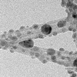
 On-wire lithography is a recently developed nanotechnology fabrication technique that allows researchers to synthesize billions of gapped nanowires with nanometer control of gap length, within a single experiment. These gaps can then be used to integrate different material segments into a single nanowire in order to fabricate functional devices. In recent work, researchers have reported a simple but efficient method to use OWL to mass produce nanotube-bridged nanowires, including carbon nanotube (CNT) channels with channel lengths as small as 5 nm. Since the CNT-bridged nanowires are comprised of CNT junctions with gold electrodes, each of the nanowires could for instance work as a CNT-based sensing device, ballistic transistors, or resonators.
Apr 5th, 2012
 OLEDs - organic light-emitting diodes - are full of promise for a range of practical applications. OLED technology is based on the phenomenon that certain organic materials emit light when fed by an electric current and it is already used in small electronic device displays in mobile phones, MP3 players, digital cameras, and also some TV screens. OLEDs in fiber form could lead to revolutionary applications by integrating optical and optoelectronic devices into textile. Combined with nanoelectronic devices, we might one day see flexible optical sensors and display screens woven into shirts and other garments. You could literally wear your next-generation smart phone or iPad on your sleeves; including the solar panels to power them.
Jan 27th, 2012
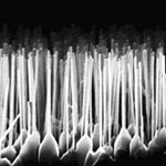
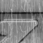 Fabrication conditions for nanoscale field-effect transistors (nano-FETs) have to meet very high requirements in order for these transistors to be used reliably as ultrasensitive and label-free molecular sensors in medical and environmental applications. Current fabrication routes for silicon-nanowire sensor construction involve high-cost, high-complexity - and often low-yield - top-down techniques such as e-beam lithography and focused ion beam. An alternative, and lower-cost, fabrication method is the use of pre-synthesized nanotubes or nanowires that are integrated into microstructures to form nano-FET sensors. Now, researchers have developed an automated vision-based nanomanipulation technique that is capable of precisely controlling the number of nanowires incorporated into each device.
Jan 24th, 2012
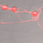 A main difference between central and peripheral nervous system is the lack of regeneration after a neurotrauma, leading to severe and irreversible handicaps. While biomaterials have been developed to aid the regeneration of peripheral nerves, the repair of central nerves such as the optic nerval or nerve cells in the spinal cord remain a major challenge for scientists. The ability to regenerate central nerve cells in the body could reduce the effects of trauma and disease in a dramatic way and nanotechnologies offer promising routes for repair techniques. Scientists have now attempted to rescue retinal ganglion cell death and enhance their regeneration using an electrospun material made of biofunctional nanofibers.
Oct 12th, 2011
 Back in 2008 we reported on nanotechnology solution for radioactive waste cleanup, specifically the use of titanate nanofibers as absorbents for the removal of radioactive ions from water. Now, the same group that developed these nanomaterials reports in a new study that the unique structural properties of titanate nanotubes and nanofibers make them superior materials for removal of radioactive cesium and iodine ions in water. Based on their earlier work, the researchers have now demonstrated a potentially cost-effective method to remediate cesium and iodine ions from contaminated water by using the unique chemistry of titanate nanotubes and nanofibers to chemisorb these ions.
Oct 4th, 2011
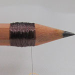 It is not often that the prefix multipliers kilo and nano come together, and when they do, it usually is in the opening chapters of physical sciences textbooks where the point is made that the universe around us spans enormous space and time scales while operating in unimaginably small ones. We are truly awestruck and inspired by the tension. Kilometer-long nanowires do have a similar eponymous echo. Researchers have now reported the first successful fabrication of arrays of millions of ordered indefinitely long nanowires and nanotubes in a flexible polymer fiber. The results are kilometer-long nanowires - a novel approach to nanowire fabrication that might bring with it fresh solutions.
Jun 23rd, 2011
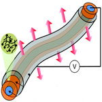
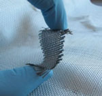 The future of your shirts, socks and gloves will be electronic. In years to come, wearable electronics will look nothing like even your smallest iPod or mobile phone today. Not only will such devices be embedded on textile substrates, but an electronics device or system could become the fabric itself. Here is some recent work that demonstrates the kind of issues scientists are working on today and that will help improve the performance of electronic textile structures. Using atomic layer deposition (ALD), researchers have grown coatings of inorganic materials on the surface of textiles like woven cotton and nonwoven polypropylene. By fabricating an all-fiber capacitor, they show that their coated materials are sufficiently conductive to perform in simple device architectures.
Jun 9th, 2011
 In a standard dye sensitized solar cell, an organic molecule adsorbed on the surface of a porous electrode absorbs light and then initiates the charge separation process eventually leading to generation of photocurrent. While the dye appears to have "sensitized" the large bandgap material, it never actually does, because only the dye molecules absorb the light and generate the carriers, the large bandgap material primarily serves the function of a conducting channel to take the electrons out. While wide bandgap materials alone can not absorb the sun light efficiently, it has been predicted that if two large bandgap materials with type-II band alignment form coaxial nanowires, the effective indirect bandgap could be substantially smaller than either of the individual materials. After a few years effort, one research team has now demonstrated a real functional device that exhibits the key feature of the idea: the use of two large bandgap materials to make a solar cell behaving like a small bandgap material.
Mar 18th, 2011
 Subscribe to our Nanotechnology Spotlight feed