MXene-enhanced hydrogel sensors for wearable technologies and human-machine interfaces
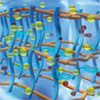 Wearable hydrogel sensors with high sensitivity and robust performance enabled by molecular design and Kirigami structures.
 Subscribe to our Nanotechnology Spotlight feed
Wearable hydrogel sensors with high sensitivity and robust performance enabled by molecular design and Kirigami structures.
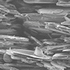 Sscientists have developed a way to strategically align microscopic heat-dissipating particles using magnetic fields, creating expressways to channel heat away from overheating electronics.
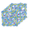
 Researchers demonstrated controllable atomic-scale patterning and resistive switching in 2D cuprous telluride crystals. Their memristor model and applications in image processing signify progress towards advanced in-memory computing.
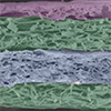
 Researchers develop a fully biodegradable and biocompatible ionotronic skin that rapidly dissolves in physiological fluids, opening the door to zero-waste wearable electronics.
 Researchers develop flexible health sensor with game-changing sensitivity. Integrating photoconductor and organic transistors enables exponential signal boost, allowing accurate continuous monitoring of heart rate, blood oxygen, blood pressure during normal daily activities.
 Researchers have developed an innovative electronic skin patch that mimics attributes of human skin for sensing biomechanical and bioelectrical signals relevant to health monitoring. The device is skin-like stretchable, breathable, and has self-adhesive properties and superior capabilities for precision mobile health tracking.
 Recent research has focused extensively on utilizing natural materials such as silk, wood, paper, plant fibers, and biomass for fabricating green electronics. These materials are abundant, low-cost, renewable, and biodegradable, making them an ideal alternative to conventional plastics.
 Researchers present the first fully roll-to-roll processed flexible Giant Magnetoresistance (GMR) thin-films with large-area deposition approach providing high-yield of magnetoresistive material.