Showing Spotlights 17 - 24 of 262 in category All (newest first):
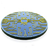
 Novel spiking neural network architecture processes images using event-driven photodetector circuits inspired by biological vision. Direct optical-to-spike conversion slashes power needs for visual pattern recognition tasks.
Feb 15th, 2024
 Researchers develop 100-nanometer-thick 'aramid nanodielectric' films ideal for skin-mounted electronics like sweat-immune medical sensors and flexible computer circuits thinner than human hair.
Jan 20th, 2024
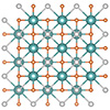 Researchers have produced exceptionally high-quality lanthanum oxychloride dielectric films perfect for constructing next-generation layered transistors compatible with two-dimensional semiconductors. The atomically smooth crystals integrate cleanly, enabling hysteresis-free switching.
Jan 19th, 2024
 Recent research realizes ferroelectric hafnium oxide memristors with ultra-low conductance and inherent current-voltage nonlinearity to mitigate limitations that have obstructed commercialization of brain-inspired neuromorphic hardware.
Jan 4th, 2024
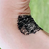 Exploring a novel method for transferring laser-induced graphene at low temperatures, vital for advancing ultrathin, flexible bioelectronics.
Dec 22nd, 2023
 Researchers accelerate the discovery of organic electronic materials through data-driven design: curating 117K compounds with quantum-predicted properties to train ML models and enable ultra-large-scale screening.
Dec 10th, 2023
 Researchers have created flexible transistors that leverage silk's nanoscale interactions with moisture to toggle between different modes of operation. The biohybrid devices act as highly sensitive breath sensors able to monitor respiratory dynamics in real time.
Oct 24th, 2023
 New perovskite technology combines light sensing and visual memory in an integrated device, emulating aspects of human vision to enable advanced artificial intelligence.
Sep 28th, 2023
 Subscribe to our Nanotechnology Spotlight feed