Showing Spotlights 57 - 64 of 262 in category All (newest first):
 Researchers have developed a method to produce a wood-derived, fully bio-based, and environmentally friendly flexible electronic circuit. They tailored the wood nanostructure to create a wood film with high transparency, flexibility, and strong mechanical properties. This material compares favorably with previously published two-dimensional cellulose-based materials developed for electronics or structural applications. This flexible circuit highlights the fact that wood can be used as a feedstock, with the potential to displace petroleum-based material for high-value products.
Mar 12th, 2020
 The goal of the electronics industry has always been to build durable devices with stable performance that last a very long time. 'Transient electronics', however, are designed with the exact opposite goal: to dissolve harmlessly into their surroundings after functioning for a certain amount of time. The fabrication process and the in vivo powering of medical implants that are only made from biodegradable materials are two of the challenges associated with transient electronics. Researchers demonstrate wirelessly powered, frequency-selective magnesium microstructures as promising candidates to be used as power receiver, microheaters and triggering elements for biodegradable implantable medical devices.
Nov 11th, 2019
 The basic idea of valleytronics is to pass information through two-dimensional (2D) and other very thin conducting materials using the energy valleys - or energy extrema - in their conduction and valence bands. Information can be transmitted by controlling an electron's association with a valley - a manipulation that can be achieved using electric fields, magnetic fields and circularly polarized light. Researchers now have demonstrated a room-temperature approach to manipulating quantum-information carriers, which is usually volatile at room temperature, in a monolayer WSe2 semiconductor.
Oct 24th, 2019
 A novel and very promising design strategy for stretchable electronics is based on liquid metals; specifically the use of the oxide shell of liquid gallium alloys to fabricate polymerized liquid metal networks (Poly-LMNs). The novel attribute of these Poly-LMNs is that they increase in conductivity as they are elongated, resulting in the measured resistance across the conductor remaining nearly unchanged as they are stretched to 700% their original length. The implication of this effect is that a circuit can now be designed with a stretchable Poly-LMN wire that won?t change its resistance when stretched.
Oct 3rd, 2019
 By studying flexible and transparent photodetectors based on single-layer MoS2 under the application of biaxial strain, researchers have developed atomically thin photodetectors whose characteristics can be controlled by means of an externally applied strain. This strain can be reversibly applied through the thermal expansion (shrinkage) of the substrate material, which induces tensile (compressive) biaxial stress. These results emphasize the possibilities of a new kind of electronics - straintronics - in which mechanical deformations are used to modify not only the geometry of the device, but its properties and performance as well.
Aug 22nd, 2019
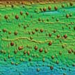
 There is a huge effort underway to use memristor devices in neuromorphic computing applications and it is now reasonable to imagine the development of a new generation of artificial intelligent devices with very low power consumption (non-volatile), ultra-fast performance and high-density integration. In new work,r esearchers were not only able to achieve to small switching effects in memristors using light, they take advantage of a percolating-like nanoparticle morphology to vastly increase the magnitude of the switching between electronic resistance states when light is incident on the device.
Jun 19th, 2019
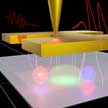 Electronic transitions between confined states within a quantum well are widely used in optoelectronics. Familiar examples include quantum cascade lasers and quantum well infrared photodetectors, which can operate in a wide range of wavelengths, from the far- to near-infrared. There is growing interest in studying this phenomenon because it may enable novel devices such as polariton lasers and because the physics of ISB polaritons is relatively unexplored. Researchers now demonstrated that it is possible to study polaritons in a single isolated nanoantenna.
Jun 18th, 2019
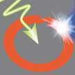
 Proton radiation damage is an important failure mechanism for electronic devices in near-Earth orbits and deep space. The future of space exploration depends crucially on the development of new electronic technologies that are immune to space radiation, which consists primarily of protons, electrons, and cosmic rays. The penetrating energetic radiation of deep space produces negative impacts on not only biological entities but also the electronic systems of space vehicles. Researchers have now demonstrated two-dimensional charge-density-wave devices with a remarkable immunity to bombardment with protons.
Apr 22nd, 2019
 Subscribe to our Nanotechnology Spotlight feed