Showing Spotlights 2529 - 2536 of 2838 in category All (newest first):
 The Oklahoma land rush of 1889 and similar land runs were events in which previously restricted land of the United States was opened for homesteading on a first come, first claim basis. A number of the individuals who participated in the run entered early and hid out until the legal time of entry to lay quick claim to some of the most choice homesteads. These people came to be identified as "sooners" and their actions led to hundreds of legal contests. Nowadays, universities and companies, from start-ups to multinational conglomerates, are rushing to aggressively stake out their turf in the nanotechnology patent area. The "sooners" in this nanotechnology patent land rush may be the ones who were issued what some say are "unduly broad" patents early on, in the hope of getting a windfall of nanotechnology intellectual property (IP) rights. While not violating the rules intentionally, upon re-examination some broad patents might not hold up to the United States Patent Act's requirement for full and complete disclosure. This uncertainty provides fertile grounds for possible litigation over nanotechnology patent claims based on broad and unprecise definitions and descriptions. Efforts are underway to address some of these problems.
May 11th, 2007
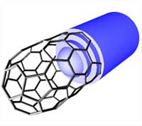 Current production methods for carbon nanotubes (CNT) result in units with different diameter, length, chirality and electronic properties, all packed together in bundles, and often blended with some amount of amorphous carbon. The separation of nanotubes according to desired properties remains a technical challenge. Especially single-walled carbon nanotube (SWCNT) sorting is a challenge because the composition and chemical properties of SWCNTs of different types are very similar, making conventional separation techniques inefficient. In order to find ways to control nanotube diameter and chirality it would be necessary to monitor nanotube growth. Then, if one knew exactly how to grow nanotubes of different characteristics, one could control their electronic properties because, depending on the way the carbon atoms are arrange around the 'waist' of a nanotube, the electronic properties could vary from metallic to semiconducting. An international group of researchers has demonstrated a novel approach to use nanotubes as reaction cells, enabling them to monitor the birth and growth of carbon nanotubes, and taking some spectacular image of this process.
May 10th, 2007
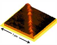 Back in 1756, the German physicist Johann Gottlob Leidenfrost published a manuscript titled De Aquae Communis Nonnullis Qualitatibus Tractatus ("A Tract About Some Qualities of Common Water") in which he described a phenomenon in which a liquid, in near contact with a mass significantly hotter than its boiling point, produces an insulating vapor layer which keeps that liquid from boiling rapidly. This effect came to be called the "Leidenfrost Effect" and the associated temperature point the "Leidenfrost Temperature." An everyday example of this can be seen in your own kitchen: sprinkle a drop of water in a hot skillet - if the skillet's temperature is at or above the Leidenfrost Temperature, the water skitters across the metal and takes longer to evaporate than it would in a skillet that is hot, but at a temperature below the Leidenfrost point. Researchers in Germany have used this effect for a novel, template-free synthesis and patterning method of nanostructures.
May 9th, 2007
 Having written in this space about the (possibly) good and the (possibly) bad of food nanotechnology before, here is now a scientific approach to assessing how the public perceives nanotechnology in food and food packaging. Swiss social psychologist Michael Siegrist has looked into the issues of trust, risk and the public acceptance of nanotechnology before. Now, he and his colleagues have taken the area of nanofoods and tried to understand what factors influence the willingness to buy food that has been produced, processed or packaged with nanotechnology. Their conclusion: Perceived benefits seems to be the most important predictor for willingness to buy.
May 8th, 2007
 For centuries, man has searched for miracle cures to end suffering caused by disease and injury. Many researchers believe nanotechnology may be mankind's first "giant step" toward this goal. Whether these beliefs are based on facts or hope, many corporations and governments are willing to invest a great deal of money to find out what happens when nanotechnology is used for medical applications - the emerging field of nanomedicine. Hundreds of millions, if not billions of dollars have been invested by governments, such as the U.S. National Cancer Institute, and the private sector in nanomedicine research and nanotech-related life sciences ventures. The 2008 budget of the U.S. National Nanotechnology Initiative provides more than $200 million for the National Institutes of Health. The European Union, particularly Germany and the UK, and Japan are also investing heavily in this field. It is difficult to find fault with a technology that promises to cure cancer almost before it starts and prevent the spread of AIDS and other infectious diseases. Scientists around the globe are searching for ways to exploit nanoparticles to improve human health. However, there are toxicological concerns and ethical issues that come with nanomedicine and they have to be addressed alongside the benefits.
May 7th, 2007
 Liquid crystal displays (LCD) have become an integral part of our everyday life. LCDs are everywhere, on your digital watches, cameras, iPods, laptop computers, television screens or car navigation displays. LCDs get their name from the special liquid crystal solution that is contained between two thin glass plates inside the display. Recent research findings suggest that embedding doped metal nanoparticles (MNP) in liquid crystal materials increases the performance of certain display devices. So far, however, the main problem with this approach has been that the inclusion of nanoparticles destabilizes the LC material. Researchers have now succeeded in synthesizing metal nanoparticle embedded stable liquid crystals in a single step, without using any external reducing and stabilizing agents. As a bottom-up strategy, this work is a further step towards synthesizing three-dimensional macro structures using small nanoparticles as building blocks, and an elegant method in fabricating soft organic architectures; particularly when it is combined with electronic, magnetic or photonic properties of inorganic materials.
May 4th, 2007
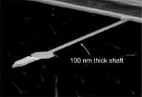 Magnetic resonance imaging (MRI) is a powerful imaging technology that serves as a non-invasive method to render images of the inside of an object. It is primarily used in medical imaging to demonstrate pathological or other physiological alterations of living tissues. MRI also has uses outside of the medical field, for instance as a non-destructive testing method to characterize the quality of products such as produce and timber. Conventional MRI usually operates at the scale of millimeters to micrometers - 3 micrometers at best - which is good enough for the mostly medical diagnostic purposes it is used for. Researchers have now shown that the imaging of nuclear spins using magnetic resonance, the basis for MRI, can be pushed to sub-100nm resolution into the nanoscale realm. They demonstrated that using an emerging technique based on force detection, they can image nuclear spins with a sensitivity that is 60,000 times better than MRI. The resolution is about 30 times better than the most advanced conventional MRI imaging. By improving this technique, researchers will be able to push deeper into the nanometer regime and approach the capability needed for direct three-dimensional imaging of individual macromolecules.
May 3rd, 2007
 It its more than 25 years of existence, Scanning Tunneling Microscopy (STM) has predominantly brought us extremely detailed images of matter at the molecular and atomic level. STM - not to be confused with the scanning electron microscope (SEM) - is a non-optical microscope that scans an electrical probe over a surface to be imaged to detect a weak electric current flowing between the tip and the surface. The STM allows scientists to visualize regions of high electron density and hence infer the position of individual atoms and molecules on the surface of a lattice. Researchers have now taken a further step by using STM to perform real-time single-molecule imaging of an entire chemical reaction. Many chemical reactions are catalyzed by metal complexes, and insight into their mechanisms is essential for the design of future catalysts. These new findings have demonstrated that the STM approach to studying chemical reactions in a dynamic environment can provide valuable information about reaction mechanisms and rates, as well as catalyst activity and stability.
May 2nd, 2007
 Subscribe to our Nanotechnology Spotlight feed