Showing Spotlights 2521 - 2528 of 2838 in category All (newest first):
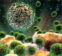 In our May 7 spotlight "The potential and the pitfalls of nanomedicine" we took a general look at the potential implications of nanomedicine and addressed some ethical issues that arise as the technology develops. In part two of this article we now take a closer look at emerging nanomedical techniques such as nanosurgery, tissue engineering, nanoparticle-enabled diagnostics, and targeted drug delivery. Again, the ethical issues inherent in these emerging medical technologies need to be considered. There are established principals for ethical assessment of existing, conventional, medical technologies and a new research article examines if and how these principals can be extended to nanomedicine.
May 23rd, 2007
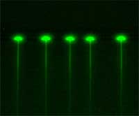
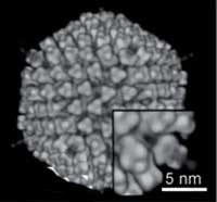 There are quite a number of terms such as bionics, biomimetics, biognosis, biomimicry, or even 'bionical creativity engineering' that refer to more or less the same thing: the application of methods and systems found in nature to the study and design of engineering systems and modern technology. A relatively new entry in this list is 'nanomimetics', an area of biomimetic nanotechnology that tries to duplicate what nature has been doing for billions of years on this planet - creating and manipulating complex nanoscale structures. Nanoscientists and nanotechnology researchers use the terms 'self-assembly' and 'bottom-up fabrication' in their efforts to copy the best nanotechnologist around - Mother Nature. Managing another small step in this direction, researchers now have reported the accurate replication of fragile biological nanoscale shapes normally associated with self-assembly by using a robust top-down lithographic technology. The ability to replicate biological shapes with nanoscale precision could have profound implications in tissue engineering, cell scaffolding, drug delivery, sensors, imaging, and immunology.
May 22nd, 2007
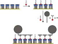 In 2005, researchers in the Netherlands developed the concept of a "molecular printboard" (named for its parallels with a computer motherboard) - a monolayer of host molecules on a solid substrate on which guest molecules can be attached with control over position, binding strength, and binding dynamics. Molecules can be positioned on the printboard using supramolecular contact printing and supramolecular dip-pen nanolithography. In this way, nanoscale patterns can be written and erased on the printboard. This technique, which combines top-down fabrication (lithography) with bottom-up methods (self-assembly), has now been applied to proteins. The resulting "protein printboards", allowing the capture and immobilization of proteins with precise control over specificity, strength and orientation, allows the fabrication of protein chips for applications in proteomics. They will play a major role in unraveling the human protein map, just as special chips were instrumental in mapping human DNA.
May 21st, 2007
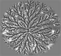 Throughout human history, technologies usually involved some kind of "top-down" approach, whether it was breaking a stone axe from a larger rock or using micro- or nanolithography to etch smaller structures from larger entities. In contrast, the self-assembly of nano-objects is an example of the principally new "bottom-up" technological approach which soon may provide novel fabrication processes and products with drastically improved properties. In particular the self-assembly of colloidal nanocrystals makes it possible to obtain structures with a high level of ordering and permit construction of patterns to be used in optoelectronics, photonics and biosensing. What makes nanocrystals so attractive to researchers is the fact that the properties essential to allow the arrangement process, including their size, shape, surface protection, stabilization and charge, can be controlled along with the electronic structure of each nanocrystal. As an example, we developed a "lab-in-a-drop" technique where a variety of nanostructures with desired properties may be produced.
May 18th, 2007
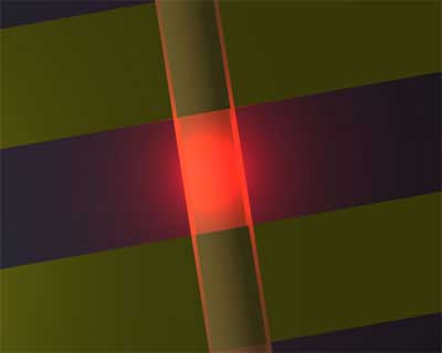
 Nanofluidic channels, confining and transporting tiny amounts of fluid, are the pipelines that make the cellular activities of organisms possible. For instance, nanoscale channels carry nutrients into cells and waste from cells. Researchers are trying to mimic Nature by constructing nanochannels in order to be able to manipulate single molecules in, predominantly biomedical, applications. Although nanochannels adjustable in size are prevalent in Nature, it is challenging to fabricate them artificially because of conflicting requirements for rigid structural integrity (to prevent collapse) on one hand and reconfigurability of nanometer-sized features on the other (to allow adjustability). Recent work at the University of Michigan addresses these issues and introduces methods to rapidly prototype structurally stable yet reconfigurable nanochannels. By fabricating tuneable elastomeric nanochannels for nanofluidic manipulation, the researchers were able to properly balance the need for flexibility and rigidity.
May 17th, 2007
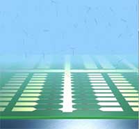 Over the next few years, semiconductor fabrication will move from the current state-of-the-art generation of 90 nanometer processes to the next 65 nm and 45 nm generations. Intel is even already working on 32 nm processor technology, code-named "Westmere", that is expected to hit the market sometime around 2009. The result of these efforts will be billion-transistor processors where a billion or more transistor-based circuits are integrated into a single chip. One of the increasingly difficult problems that chip designers are facing is that the high density of components packed on a chip makes interconnections increasingly difficult. In order to be able to continue the trend predicted by Moore's law, at least for a few more years, researchers are now turning to alternative materials for transistors and interconnect and one of the prime candidates for this job are single-walled carbon nanotubes (SWCNT). However, one of the biggest limitations of conventional carbon nanotube device fabrication techniques today is the inability to scale up the processes to fabricate a large number of devices on a single chip. Researchers in Germany have now demonstrated the directed and precise assembly of single-nanotube devices with an integration density of several million devices per square centimeter, using a novel aspect of nanotube dielectrophoresis. This development is a big step towards commercial realization of CNT-based electronic devices and their integration into the existing silicon-based processor technologies.
May 16th, 2007
 Integrating biochemical analysis with micro- and nano-oelectromechanical systems (MEMS and NEMS) has led to the development of a new class of biomedical analytical devices called lab-on-a-chip. They combine a number of biological functions (such as enzymatic reactions, antigen-antibody conjugation, and DNA probing) with proper micro- or even nanofluidic laboratory components (such as sample dilution, pumping, mixing, metering, incubation, or separation) and detection in micron- and nanometer-sized channels and reservoirs into one single device. In order to reduce the size of these lab-on-chip devices even more, researchers increasingly are finding ways to turn micron-sized components into nanosized components. One problem they have been faced with so far is the issue of illumination. Today, many state-of-the-art lab-on-a-chip devices use external illumination sources, such as lasers or light emitting diodes (LEDs). Being able to fully integrate the excitation and detection mechanisms on lab-on-a-chip devices would allow further size reductions and increase the flexibility for using and handling them. Researchers at Cornell University have electrospun light-emitting nanofibers that, if they can be integrated with micro- and nanofluidic devices, could achieve excitation of light-induced fluorescence and detection within that same device.
May 15th, 2007
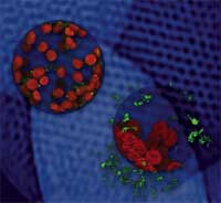 Most nanobiotechnology research today is focused on human medical applications and, mostly for testing and demonstration purposes, on animals. As nanotechnology is gaining interest with regard to agricultural applications, plant science research focusing on investigation of plant genomics and gene function as well as improvement of crop species has become a nanotechnology frontier. Plant cells differ from animal cells in several aspects, a major one being that they possess a wall surrounding them to provide, among other things, mechanical and structural support. The plant cell wall is generally made up of pollysacharides and cellulose. Cellulose provides a stiff and rigid environment for the cell to live in. Thanks to this wall, viruses have no active way of penetrating plant cells but rely on mechanical wounds or infected seeds for transmission. Researchers are commonly using surface-functionalized silica nanoparticles as nonviral nanocarriers for experimental drug and DNA delivery into animal cells but their use with plants so far was limited due to the cell wall. In a first demonstration of the utilization of porous nanoparticle materials for intracellular controlled release and gene transfer application in plants, researchers have used silica nanoparticles to penetrate the cell wall and deliver a payload into the cell.
May 14th, 2007
 Subscribe to our Nanotechnology Spotlight feed