Showing Spotlights 2537 - 2544 of 2838 in category All (newest first):
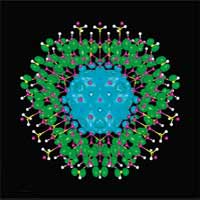
 Currently, the most common carrier vehicles to deliver therapeutic drugs, genes or proteins to a patient's target cells are viruses that have been genetically altered to carry the desired payload. These viruses infect cells, deposit their payloads, and take over the cells' machinery to produce the desirable proteins. One problem with this method is that the human body has developed a very effective immune system that protects it from viral infections and another problem is that viral-based delivery vehicles may integrate into the host genome. Thanks to advances in nanotechnology fabrication techniques, the development of nonviral nanocarriers for gene and drug delivery has become possible. Besides viruses, polymeric systems and various inorganic nanomaterials are under intensive investigation as nonviral delivery vehicles. Finding new candidates for vehicles is still of great interest because most existing synthetic vehicles exhibit intrinsic cytotoxicity and show relatively low delivery efficiency. Enter the carbon nanohorn (CNH). This recently recognized member of the fullerene family has a unique dahlia flower-like structure, huge surface areas and can be fabricated with high purity. Researchers believe that CNHs may have potential advantages over normal nanoparticles, nanorods and nanotubes as synthetic intracellular delivery vehicles.
May 1st, 2007
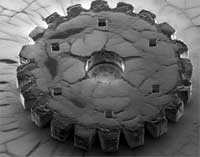
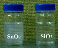 One of the newly emerging areas of semiconductor technology is the field of transparent electronics. These thin-film materials hold the promise of a new class of flexible and transparent electronic components that would be more environmentally benign than current electronics. Being able to print transparent circuits on low-cost, flexible, plastic substrates opens up the possibility of a wide range of new applications, ranging from windshield displays and flexible solar cells to clear toys and artificial skins and even sensor implants. It is likely that such flexible see-through structures will find wide uses in military, biosensing and consumer goods due to the advantages of high transparency and reliable electrical characteristics. However, the emerging transparent electronics technology is facing manufacturing problems: current fabricating processes do not separate the device manufacturing from material synthesis. The transparent electronic materials, which are largely inorganic oxides. are directly deposited on the device substrate under harsh conditions which may cause damage to the existing layer or flexible substrate. The etching of small dimension oxide multilayer is also difficult due to the low selectivity of the etching recipe. New research results demonstrate that nanofabrication techniques could solve these problems.
Apr 30th, 2007
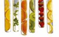 Nanotechnology has begun to find potential applications in the area of functional food by engineering biological molecules toward functions very different from those they have in nature, opening up a whole new area of research and development. Of course, there seems to be no limit to what food technologists are prepared to do to our food (read this delightful romp through the food processing industry to get the idea: "Twinkie, Deconstructed". For the non-U.S. reader: a Twinkie is a processed foodlike substance that has reached iconic status in this country) and nanotechnology will give them a whole new set of tools to go to new extremes. We have taken a critical view of food nanotechnology before in this column and in our news coverage, just take a look at "Nanotechnology food coming to a fridge near you" or "Are you ready for your nano-engineered wine?". Today, though, we look at the potentially beneficial effects nanotechnology-enabled innovations could have on our foods and, subsequently, on our health.
Apr 27th, 2007
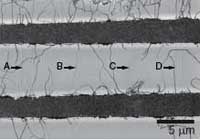 Synthesis of carbon nanotubes (CNTs) is a rapidly advancing field, but there is a lot that researchers don't know about how nanotubes form and grow. Synthesis, while rapidly developing, is currently the weakest link for most nanotube applications, with high yield and high precision diameter and chirality control being important goals. Historically, in situ characterization tools have accelerated progress in synthesis for many advanced materials, and there is widespread recognition that in situ tools have the potential to improve CNT synthesis as well. Ideally one would like to detect individual nanotubes and ensembles as they grow and measure their physical properties while imposing minimal constraints on the synthesis method. In other words, with a good understanding of the synthesis process we would be better able to control the product. It is feasible that by actually observing nanotubes as they grow one will gain a better understanding of the growth process and also better characterize the grown product. Greater control over the physical characteristics of the nanotube product is essential to enable many applications, as well as many fundamental studies. Although chemical vapor deposition (CVD) is now a very standard method to synthesize CNTs, there aren't really standard in situ tools to characterize nanotubes during growth. Researchers in Canada have now shown how global Raman imaging (GRI) can be used to characterize the CVD growth of CNTs in situ and in real time.
Apr 26th, 2007
 The promise of revolutionary bottom-up nanotechnology is based on a vision of molecular assembly technologies where nanoscale materials and structures self-assemble to microscale structures and finally to macroscopic devices and products. We are a long way from realizing this vision but researchers are busily laying the foundation for the things to come. Assembling nanoscopic components into macroscopic materials has been an appealing goal but one of the enormous difficulties lies in bridging approximately six orders of magnitude that separate the nanoscale from the macroscopic world. New research at Northwestern University in the U.S. helps to overcomes this difficulty by dividing the assembly process into two manageable sub-steps. First, nanoparticles are assembled into larger, 100 nm-size, spherical building blocks, which are both deformable and "sticky" towards one another. Once assembled, these components "glue" together like pieces of clay to give millimeter or even centimeter-sized structures. The novelty of this technique is both the hierarchical assembly approach (i.e., atoms to nanoparticles to supraspheres to macroscopic materials) and the resulting "soft" structures, which contrast with previously reported hard and brittle nanoparticles assemblies/crystals. This research takes a further step in making nanoscale discoveries relevant to our everyday - macroscopic - world.
Apr 25th, 2007
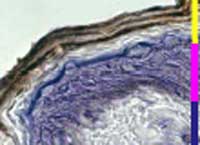 Engineered nanoparticles are at the forefront of the rapidly developing field of nanomedicine. Their unique size-dependent properties, of which optical and magnetic effects are the most used for biological applications, makes them suitable for a wide range of biomedical applications such as cell labeling and targeting, tissue engineering, drug delivery and drug targeting, magnetic resonance imaging, probing of DNA structure, tumor destruction via heating (hyperthermia), and detection and analysis of biomolecules such as proteins or pathogens. Many of these applications can also be tailored to target skin to help in the early diagnosis of a skin disease, which then could also be treated via nanocarriers. In addition, a tissue engineering approach could be useful for skin wound healing therapies and the magnetic properties of these particles might help in directing and localizing these agents in a particular layer of the skin where their action is desired. Unfortunately, if nanoparticles are able to penetrate layers of skin for therapeutic purposes, they might equally be able to penetrate skin unintentionally. This raises the question if people, who are exposed to such nanomaterials, could accidentally be contaminated and thus exposed to a potential local and/or systemic health risk. Researchers in Italy now have begun to systematically evaluate both risks and applications of nanoparticle skin absorption.
Apr 24th, 2007
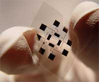 The fabrication of electronic devices on plastic substrates has attracted considerable recent attention owing to the proliferation of handheld, portable consumer electronics. Plastic substrates possess many attractive properties including biocompatibility, flexibility, light weight, shock resistance, softness and transparency. Achieving high performance electronics or sensors on plastic substrates is difficult, because plastics melt at temperatures above 120 degrees C. Central to continued advances in high-performance plastic electronics is the development of robust methods for overcoming this temperature restriction. Unfortunately, high quality semiconductors (such as silicon) require high growth temperatures, so their application to flexible plastics is prohibited. A group of researchers at the California Institute of Technology now showed that highly ordered films of silicon nanowires can be literally glued onto pieces of plastic to make flexible sensors with state-of-the-art sensitivity to a range of toxic chemicals. These nanowires are crystalline wires made out of doped silicon - the mainstay of the computer industry. By etching nanowires into a wafer of silicon, and then peeling them off and transferring them to plastic, they developed a general, parallel, and scalable strategy for achieving high performance electronics on low cost plastic substrates.
Apr 23rd, 2007
 Nanowires have received a great deal of interest in recent years. As quasi one-dimensional systems they may overcome the fundamental difficulty in the electronic transport encountered when attempting to use quasi zero-dimensional structures (quantum dots) while still being able to take advantage of the effects related to quantum confinement. In a conventional semiconductor, electrons and holes typically stay in the same region after photoexcitation, which is very desirable for certain applications, light-emitting devices for instance. However, for a number of key renewable energy applications, including hydrogen generation via photoelectrochemical water splitting, dye-sensitized solar cells, and even regular solar cells, the efficient charge separation of the electron and hole after photoexcitation is instead highly preferred, although not readily available in the existing repertory of materials. In this context, researchers have explored the use of core-shell nanowires for such applications. However, for the material combinations that have been investigated, the energy alignments between the core and the shell are typically type I, and thus, the role of the shell is to either provide quantum confinement to both electrons and holes in the core or a protective cladding to the core to reduce sensitivity to the environment. Researchers at the National Renewable Energy Laboratory and Lawrence Berkeley National Laboratory designed a new class of core-shell semiconductor nanowires with strong type II band alignments. The photo-generated electron and hole in such nanowires are naturally separated in the core and shell, respectively, making them much more suitable for the solar energy applications than type I core-shell nanowires.
Apr 20th, 2007
 Subscribe to our Nanotechnology Spotlight feed