Showing Spotlights 2433 - 2440 of 2838 in category All (newest first):
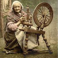 Modern nanotechnology researchers not only borrow extensively from nature to develop new materials and fabrication techniques, they also manage to transfer proven, and sometimes ancient, technologies into their nanotechnology laboratories. We've written about this before in our stories about welding ("Bronze Age technique works just fine in the nanotechnology era") and metal forging ("From Bronze Age shack to nanotechnology lab - metal forging techniques reach the bottom"). Today, our story deals with yet another ur-technology: spinning. Spinning is the process of creating yarn (or thread, rope, cable) from various raw fiber materials. The first spinning wheel was invented in India probably some 2,500-3,000 years ago, although some claim that the Chinese used similar devices as long as almost 5,000 years ago to spin silk threads. While spinning is one of the core technology foundations of our civilization, researchers have now begun to apply cotton-spinning techniques to fabricate carbon nanotube (CNT) "yarn."
Oct 4th, 2007
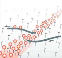 Shuttles - whether the space shuttle, an airport shuttle bus, or a loom shuttle - basically do one thing: they transport cargo (astronauts, passengers, thread) from one point to another on a controlled route. Although not always called shuttles, the basic concept is critical to modern transportation systems and is used by nearly every society. The concept of the shuttle has been used for centuries from Egyptian barges to Roman railways and canals. Even before these inventions, however, nature employed molecular shuttles in biological organisms. In molecular shuttles, kinesin proteins propel cargo (such as organelles) along hollow tubes called microtubules. Cells use these motors to transport cargo to highly specific destinations, in order to regulate levels of macromolecules and processes, much like a train along a track. Using biological motors to transport and precisely distribute cargo requires a clear understanding of how molecular shuttles pick up and deliver specific payload. However, scientists are challenged by the need to better control the interactions along the route so that the cargo remains on the line when not needed, but when it is needed, can be picked up and transported to a specific location. Researchers in Switzerland have now built nanoscale cargo loading stations and shuttles, an important step towards assembly lines for nanotechnology.
Oct 3rd, 2007
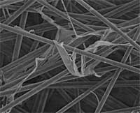
 The need for 3D visualization and analysis at high spatial resolution is likely to increase as nanoscience and nanotechnology become increasingly important and nanotomography could play a key role in understanding structure, composition and physico-chemical properties at the nanoscale. Scientists from the Electron Microscopy Group at the University of Cambridge in the UK report that nanotomography is becoming an important tool in the study of the size, shape, distribution and composition of various materials, including nanomaterials.
Oct 2nd, 2007
 In our Spotlight from a few weeks ago - Nanopyramids - temporary resting places for light - we wrote about things like Q-factors, qubits, stopping light and other fascinating concepts and emerging techniques that could lead to quantum computing. Some of the feedback we received could be summarized with "Huh? Q-what...?" So today we'll take another look at the Quality (Q) factor of photonic-crystal nanocavities and the context it is relevant in. These 'nanocages' for light are currently the focus of much interest of nanotechnology research in photonics because they can strongly confine photons in a tiny space. Just as semiconductor crystals control the flow of electrons (the basis for all electronics), photonic crystals are a unique material used to construct photonic devices and circuits for manipulating light, i.e. photons. A prominent example of a photonic crystal is the naturally occurring gemstone opal. Photons (behaving as waves) propagate through it - or not - depending on their wavelength. Wavelengths of light (stream of photons) that are allowed to travel throught he crystal are known as "modes". Disallowed bands of wavelengths are called photonic band gaps. What's so interesting for researchers is that, once you are able to fully control and manipulate photons, you could not only vastly improve existing applications like optical data storage, high-precision sensing and telecommunications, but develop exotic technologies like quantum computing.
Oct 1st, 2007
 Every few months you can read about a recall of food items, be it fresh spinach of bottled infant formula, due to contamination with salmonella, E. coli or some other foodborne pathogen. A pathogen is a an organism that causes disease in another organism. The Centers for Disease Control and Prevention (CDC) estimates that foodborne diseases cause 76 million illnesses, 325,000 hospitalizations, and 5,000 deaths each year. In 2000, the U.S. Department of Agriculture (USDA) estimated the costs associated with five major bacterial foodborne pathogens to be $6.9 billion. The Food and Drug Administration's 2005 Food Code states that the estimated cost of foodborne illness is $10-$83 billion annually. These staggering numbers, not to mention the potential of foodborne pathogens for terrorists attacks, are driving the development of biosensors as important analytical tools for the rapid detection of pathogens in the field, and they are increasingly playing a key role in controlling disease outbreaks. Immunosensors (biosensors that use antibodies as biological recognition elements) are of great interest because of their applicability (any compound can be analyzed as long as specific antibodies are available) and high sensitivity. High sensitivity, of course, is an important attribute in designing biosensors, but a large variance due to stochastic interaction between biomolecules, biosensor imperfections, and environmental variability (e.g., pH of the analyte) directly affects the reliability of the measured signal in almost all sensors. Researchers have now taken forward error-correction (FEC) techniques, already successfully applied for improving reliability of communication and storage systems such as CDs, and applied them to biosensors.
Sep 28th, 2007
 Yesterday we wrote about air bridges in nanotechnology fabrication. Today we show a practical example. Traditionally, electronic devices have been fabricated by top-down fabrication methods. Conducting polymers, for instance, have been synthesized as micro- and nanoscale fibers, tubes and wires for more than 10 years now. More recently, nanowires have been integrated into electronic circuits, making possible the development of devices such as polymer nanowire chemical sensors with superior performance. What most of these fabrication techniques have in common is that they are template-based (e.g. lithography or DNA templates) or depend on specialized fiber forming techniques such as electrospinning. However, as electronic components become smaller and smaller it is increasingly more difficult to use existing methods of fabrication. New methods must be developed. A group of researchers in Australia have demonstrated a technique for growing ordered polymer nanowires within a pre-patterned electronic circuit such that electrical contacts to the nanowires are made in situ during the growth procedure, avoiding the time-consuming and challenging task of manipulating nanowires into position and making electrical contacts post-synthesis.
Sep 27th, 2007
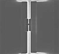
 Bridges are exciting to cross, incredible works of engineering and they have made it possible for us to travel more easily, quickly and safely. The U.S. Congress even approved $400 million to build a bridge to nowhere. While bridges have been, and still are, essential components in every society's infrastructure, the bridge concept is becoming interesting to nanotechnology researchers as well. Nanomaterial air bridges enable nanoscale structures to be suspended as a two-point beam, creating a nanomechanical element that is isolated from a variety of substrate effects, including adhesion, temperature, conductivity, and parasitic capacitance. The bridge-like suspension makes nanoscale structures accessible along their length, which is beneficial for examining ehmt but also for device construction. It also allows nearfield probing, manipulation, and actuation of these suspended nanostructures. Scientists at the University of Louisville have found a way to build nanomaterial air bridges simply and conveniently.
Sep 26th, 2007
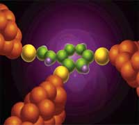 Transistors are the fundamental building blocks of our everyday modern electronics; they are the tiny switches that process the ones and zeroes that make up our digital world. Transistors control the flow of electricity by switching current on or off and by amplifying electrical signals in the circuitry that governs the operation of our computers, cellular phones, iPods and any other electronic device you can think of. The first transistor used in commercial applications was in the Regency TR-1 transistor radio, which went on sale in 1954 for $49.95, that's over $375 in today's dollars (for everyone in the iPod generation - watch this fascinating 1955 video clip artifact how the first transistor radio was hand built). While the first transistors were over 1 centimeter in diameter, the smallest transistors today are just 30 nanometers thick - three million times smaller. This feat would be equivalent to shrinking the 509-meter tall Taipei 101 Tower, currently the tallest building in the world, to the size of a 1.6 millimeter tall grain of rice. The 32nm microprocessor Intel plans to introduce in 2009 will pack a whopping 1.9 billion transistors. However, current microprocessor technology is quickly approaching a physical barrier. Switching the current by raising and lowering the electron energy barrier generates heat, which becomes a huge problem as device densities approach the atomic limit. An intriguing - and technologically daunting - alternative would be to exploit the wave nature of the electron, rather than its particle properties, to control current flow on the nanoscale. Such a device, called the Quantum Interference Effect Transistor (QuIET), has been proposed by researchers in Arizona. This device could be as small as a single benzene molecule, and would produce much less heat than a conventional field effect transistor.
Sep 25th, 2007
 Subscribe to our Nanotechnology Spotlight feed