Showing Spotlights 2425 - 2432 of 2838 in category All (newest first):
 Nanoelectronics deals with functional electron devices, such as transistors, in the nanoscale range size. As the name implies, nanoelectronics runs on electricity, i.e. the transport of electrons. Another approach to creating faster,smaller and more energy-efficient electronics is to move the field of optical information processing towards the nanoscale. Optical nanoelectronics will work with light instead of electron transport. Here the usual circuit elements such as inductors, capacitors and resistors could be created in order to operate using infrared or visible light. Using nanotechnology, researchers are able to create structures that could operate on the same or smaller scale as the wavelength of light (the wavelength of visible light is roughly between 400 and 700 nanometers). Going beyond 'conventional' nanoelectronics, researchers have now proposed a form of optical circuitry in which a network of subwavelength nanoscale metamaterial structures and nanoparticles may provide a mechanism for tailoring, patterning, and manipulating optical electric fields in a subwavelength domain, leading to the possibility of optical information processing at the nanometer scale.
Oct 16th, 2007
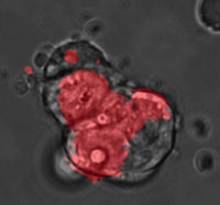 A quantum dot (QD), also called a nanocrystal, is a semiconductor nanostructure that can be as small as 2 to 10 nm. The usefulness of quantum dots comes from their peak emission frequency's extreme sensitivity - quantum mechanical in nature - to both the dot's size and composition. QDs have been touted as possible replacements for organic dyes in the imaging of biological systems, due to their excellent fluorescent properties, good chemical stability, broad excitation ranges and high photobleaching thresholds. By contrast, conventional organic dyes cannot be easily synthesized to emit different colors and have narrow excitation spectra and broad emission spectra that often cross into the red wavelengths, making it difficult to use these dyes for multiplexing. QDs hold increasing potential for cellular imaging both in vitro and in vivo. Researchers have now used QDs for in vivo imaging of embryonic stem cells in mice. This opens up the possibility of using QDs for fast and accurate imaging applications in stem cell therapy.
Oct 15th, 2007
 Medicine is big business. The big pharma companies have traditionally enjoyed enormous profits that would make the eyes of other companies' CEOs water (apart from big oil companies, of course). The combined annual net income for the top 10 pharma companies (ranked by market capitalization) currently is about $73 billion. Pfizer alone has a net income of approximately $19 billion. The recipe for success? Patent protection and intellectual property rights (IPRs). The core of Big Pharma's business model relies on patent protection for their blockbuster drugs, which allows them to sell these drugs at extraordinarily high profit margins that they wouldn't be able to generate in a competitive market. Point in case: Lipitor, the cholesterol-lowering drug that accounts for nearly $13 billion of Pfizer's revenues and over 40% of its profits. Another key part of the pharma business model is heavy spending on sales and marketing. Novartis, for instance, is spending around 33% of sales on promotion, compared with about 19% on R&D, although the cost of bringing a new drug to market could well exceed $1 billion (and that is also the argument pharma companies use to justify their profits). However, pharmaceutical companies are faced with the expiration of the patent protection on their main profit generators, they have relatively few new products in the pipeline, and they need to come to terms with the emerging nanomedicine landscape. While nanomedicine potentially offers promising new value propositions and revenue streams, for instance in diagnostics, it also could completely displace certain classes of drugs such as current chemotherapy agents with novel nanoparticle reformulations. In what looks like more of the same though, it seems that the future of nanomedicine business will also depend on patents and IPRs, potentially even more so than today.
Oct 12th, 2007
 The problem with most current hydrogen sensor designs is that they are built on rigid substrates, which cannot be bent, and therefore, their applications might be limited due to the mechanical rigidity. In addition, they use expensive, pure palladium. A new type of sensors is bendy and use single-walled carbon nanotubes to improve efficiency and reduce cost. In the example of the space shuttle, laminating a dense array of flexible sensors on the whole surface of a pipe can detect any leakage of hydrogen prior to diffusion and alert control units to remedy the malfunction.
Oct 11th, 2007
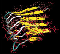 Nature is truly a brilliant nano engineer and has been so for billions of years. There is an abundance of 'smart' biological materials with hierarchical nanostructures - built from proteins - that are capable of adapting to new tasks, are self-healing, and can self-assemble autonomously simply out of a solution of building blocks. The performance and capability of these natural materials is something engineers can only dream of today. But by unlocking nature's secrets tiny step by tiny step, one day we will be able to not only duplicate but surpass the performance of natural materials. Only in recent years have scientists begun to understand the underlying principles and mechanisms of these materials - Why is spider silk stronger than steel? Why can cells be stretched reversibly several times of their original length? What kinds of molecular flaws lead to malfunctions in cells and tissues, as it occurs in Alzheimer's, rapid ageing disease progeria or muscle dystrophies, diseases in which the cell or tissue fails mechanically? Scientists at MIT have, for the first time, revealed the fundamental fracture and deformation mechanisms of biological protein materials, clarifying some long-standing issues about the deformation behavior of cells and Alzheimer's pathogens. The researchers report that the fracture mechanisms of two abundant nanoscopic building blocks of many proteins and protein materials exhibit two distinct fracture modes, depending on the speed of deformation. This is a surprising observation with far-reaching implications for the development of novel self-assembled protein materials and possibly the cure of certain genetic diseases
Oct 10th, 2007
 In an earlier Spotlight we reported on NIOSH's Nanotechnology Research Center (NTRC) and its efforts concerning the occupational safety and health perspectives of engineered nanomaterials (Nanotechnology in the workplace). Today, we are looking at the specific steps undertaken by companies active in the field. "We were receiving a steady stream of questions from industry and academia regarding what we knew about the hazards of nanomaterials," Charles L. Geraci, Branch Chief at the National Institute of Occupational Safety and Health (NIOSH) and Co-Coordinator of the NIOSH Nanotechnology Field Team, tells Nanowerk. "People were coming to NIOSH for recommendations; we knew we needed to have a better understanding of the nature of workplace exposure during research, production and use." But, in a new and relatively little studied area of industry, where does one find these answers? NIOSH already had a strong research program to address questions in the lab, says Geraci, but field data was needed to have a complete picture. "In our minds, the best way to achieve this was to do what NIOSH does best: get in the field and gather data through observation and measurement." In 2006, the concept of a field team dedicated to this effort was developed.
Oct 9th, 2007
 Nanoimprint lithography (NIL) has developed into a key technique for the fabrication of polymer nanopatterns and three-dimensional (3D) nanostructures. At its core, NIL is a simple nanometer scale pattern transfer process where a master mold with a desired pattern is used to fabricate identical patterns in an imprint resist, typically a polymer, with subsequent heat or light curing of the resulting mold. The attractivity of NIL comes from its capability for patterning with high resolution, high fidelity, high throughput, and low cost. Using NIL, nanometer sized patterns can easily be formed on various substrates, including silicon wafers, glass plates, flexible polymer films, and even nonplanar substrates. The limitation of conventional NIL techniques lies in their resulting patterned 2D layers; the formation of 3D micro- and nanostructures by stacking the 2D layers cannot be achieved by conventional NIL. That's why researchers came up with reverse nanoimprint lithography, a technique to transfer patterned 2D layers and to form multistacked 3D micro- and nanostructures on the substrate. While this works in principal, the achievable yields are very low due to the difficulty of detaching the master mold from the 3D structure. Researchers in South Korea have now managed to demonstrate the first successful fabrication of multi-stacked 2D nano patterned slabs on various substrates including flexible polymer film. This means real 3D nano structures such as photonic crystals can be fabricated with reasonable cost.
Oct 8th, 2007
 Individual nanoscale building blocks, such as nanoparticles, nanosheets, nanowires or nanotubes display unique and unusually impressive mechanical properties. These mechanical properties of nanomaterials cannot be extrapolated from their bulk properties and scientists are still busily exploring the nanoscale behavior of various materials. Once the nanoscale properties of a material are known, the next problem is how to practically exploit certain properties and transfer them back into a macro structure of a bulk material. Materials engineers would love to transfer the exceptional mechanical properties such as tensile strength and Young's modulus (a measure of stiffness that reflects the resistance of a material to elongation) of nanoscale materials into nanocomposites that then cold be used to build much tougher, lighter and flexible materials than anything we know today - say a paper thin sheet of nanocomposite material that is transparent, flexible, yet as strong as steel. So far, effective load transfer and homogenous dispersion appear to be the key issues in order to take advantage of the extraordinary properties of nanomaterials for mechanical reinforcement applications. New research coming out of the University of Michigan has resulted in nanocomposite materials with a very high content of inorganic component and nearly perfect stress transfer. The stiffness and tensile strength of these multilayer composites are an order of magnitude greater than those of analogous nanocomposites at a processing temperature that is much lower than those of ceramic or polymer materials with similar characteristics.
Oct 5th, 2007
 Subscribe to our Nanotechnology Spotlight feed