Showing Spotlights 177 - 184 of 262 in category All (newest first):
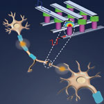 Researchers demonstrate a new single element nanoscale device, based on the successfully commercialized phase change material technology, emulating the functionality and the plasticity of biological synapses. In the nervous system, a synapse is the junction between two neurons, enabling the transmission of electric messages from one neuron to another and the adaptation of the message as a function of the nature of the incoming signal - something that is called plasticity. Synapses dominate the architecture of the brain and are responsible for massive parallelism, structural plasticity, and robustness of the brain. Therefore, a compact nanoelectronic device emulating the functions and plasticity of biological synapses will be the most important building block of brain-inspired computational systems.
Jun 21st, 2011
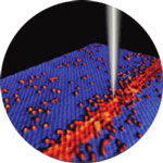 Germanium was the basic material of first-generation transistors in the late 1940s and early 1950s before it was replaced by silicon (the first silicon transistor was produced by Texas Instruments in 1954). Using germanium instead of silicon as transistor material would enable faster chips containing smaller transistors because higher switching speeds than in silicon could be achieved using germanium. A novel fabrication route demonstrated by a research team in Australia, using a combination of scanning tunneling microscope (STM) lithography and high-quality crystal growth, opens up an entire new area where quantum behavior of highly confined electrons in germanium can be studied for the first time.
May 20th, 2011
 A memristor is a two-terminal electronic device whose conductance can be precisely modulated by charge or flux through it. It has the special property that its resistance can be programmed (resistor) and subsequently remains stored (memory). It is thought memristors - with the ability to 'remember' the total electronic charge that passes through them - will be of greatest benefit when they can act like synapses within electronic circuits, mimicking the complex network of neurons present in the brain, enabling our own ability to perceive, think and remember. Researchers have now analyzed in unprecedented detail the physical and chemical properties of an electronic device that computer engineers hope will transform computing.
May 16th, 2011
 Ink-jet printing of metal nanoparticles for conductive metal patterns has attracted great interest as an alternative to expensive fabrication techniques like vapor deposition. The bulk of the research in this area focuses on printing metal nanoparticle suspensions (metallic ink) for metallization. Printing conductive features by metallic nanoparticle inks must be followed by an additional step of sintering, usually achieved by heating to elevated temperatures. In this step, the nanoparticles composing the pattern will coalesce to form a continuous electrical contact. In new work, researchers have now demonstrated a new conductive ink that won't require a post printing sintering step. It is achieved by the addition of a latent sintering agent that gets into action after the printing step. Once the solvent evaporates, the sintering agent concentration increases, leading to the spontaneous sintering of the nanoparticles.
Apr 18th, 2011
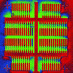 The commercial realization of carbon nanotube-based electronic devices and their integration into the existing silicon-based processor technologies is still hampered by the inability to scale up the - currently lab-based - fabrication processes to manufacture a large number of devices on a single chip. The fundamental issue of carbon nanotube device fabrication still remains the biggest challenge for effective commercialization of nanotube electronics. In a further step towards large-scale integration of single-walled carbon nanotubes (SWCNTs) into complex functional electronic circuits, researchers have now combined a previously developed dielectrophoretic deposition approach with SWCNT sorting using density gradient ultracentrifugation, ensuring high purity of SWCNTs in suspension and consequently in the assembled devices.
Mar 22nd, 2011
 Although organic semiconductor materials cannot yet be packed as densely as state-of-the-art silicon chips, they require less power, cost less and do things silicon devices cannot: bend and fold, for example. Once perfected, organic semiconductors will permit the construction of low-cost, spray-on solar cells and even spray-on video displays. Notwithstanding tremendous progress in the area of organic electronics, several major challenges still exist. To address these challenges, researchers have combined organic electronics with nanoelectronics and developed the first 2D crystal of organic semiconductors on the millimeter scale, the thickness of which is only a single molecular layer, but with perfect long-ranged crystalline order.
Mar 15th, 2011
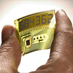 Printed electronics has its origins in conductive patterns printed as part of conventional electronics, forming flexible keyboards, antennas and so on. Then came fully printed testers on batteries, electronic skin patches and other devices made entirely by printing, including batteries and displays. A clear next step has been to modernise static print with the e-reader and the talking poster with animated, light emitting display and solar power. These are partly or almost wholly printed, with a clear roadmap to making them lower cost and more reliable and flexible by using printing more fully in their manufacture in future. However, we now see printed electronics and electrics certain to penetrate far more applications than anyone realised.
Feb 15th, 2011
 One of the many fascinating concepts in nanotechnology is the vision of molecular electronics where researchers are investigating nanostructured materials to build electronics from individual molecules. If realized, the shift in size from even the most densely packed computer chip today would be staggering. Molecular electronics aims at the fundamental understanding of charge transport through molecules and is motivated by the vision of molecular circuits to enable miniscule, powerful and energy efficient computers. A research team in Germany has now demonstrated that rigidly wired molecules can emit light under voltage bias. This result is important for fundamental science but it also adds to the molecular electronics vision an optoelectronic component, i.e. the development of optoelectronic components on the basis of single molecules.
Nov 29th, 2010
 Subscribe to our Nanotechnology Spotlight feed