Showing Spotlights 153 - 160 of 262 in category All (newest first):
 For a transistor to work properly, it must contain impurity atoms - called dopants - replacing the silicon atoms at certain places in the device. Given that modern transistor are approaching the atomic scale, the exact location of a single dopant atom becomes critical in determining the device functionality. In a different context, single dopant atoms in semiconductors have now proved to be an excellent platform to encode quantum information. Therefore, the exact location of single dopant atoms is also crucial to future quantum computers based on silicon. A new technique allows the accurate location of a single dopant atom in a nanoscale device, after the device has been fabricated, and without damaging or altering any of its functionalities.
May 8th, 2013
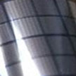 With all the rapid progress going on in research and commercialization of flexible and transparent electronics, the obvious question is not if, but when it will be possible to build a flexible and transparent truly high performance computer. A research team has now shown, for the first time, a generic batch fabrication process to obtain mechanically flexible and transparent mono-crystalline silicon (100) from bulk wafers. The researchers demonstrate a pragmatic pathway for a truly high performance computation systems on flexible and transparent platform.
Mar 1st, 2013
 The low-frequency fluctuations in electrical current attract particular attention among researchers. The low-frequency electronic 1/f noise was first discovered in vacuum tubes, in 1925, and later observed in a wide variety of electronic materials and devices. The importance of this noise for electronic and communication devices motivated numerous studies of its physical mechanisms and methods for its control. Researchers were now able to shed light on 1/f noise origin and mechanisms using a set of multi-layered graphene samples with the thickness continuously varied from around 15 atomic planes to a single layer of graphene.
Feb 27th, 2013
 The coming age of wearable, highly flexible and transparent electronic devices will rely on essentially invisible electronic and optoelectronic circuits. In order to have close to invisible circuitry, one must have optically transparent thin-film transistors. In order to have flexibility, one needs bendable substrates. Researchers have now now fabricated transistors on specially designed nanopaper. They show that flexible organic field-effect transistors (OFETs) with high transparency and excellent mechanical properties can be fabricated on tailored nanopapers.
Feb 21st, 2013
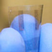
 Chemical and analytical processes using channel-based microfluidics have many advantages, such as the reduced use of chemical reagents and solvents; precisely controlled reaction condition; much shortened reaction time; and the ability to integrate into a digital device. However, it is difficult with channel microfluidics to handle just a single droplet. In contrast with the microchannel-based fluidics, the manipulation of discrete droplets without using channels is a new field. Here, a liquid droplet is not confined to a closed channel and there is no risk of it being adsorbed on a channel wall. A 'liquid marble' coated with micro- or nanoparticles is a novel kind of microfluidic device, one that is especially useful for handling single liquid droplet. Researchers have now come up with the idea of developing 'liquid metal marbles' when they wanted to develop a flexible conductive system for electronic and electromagnetic units.
Aug 20th, 2012
 Thanks to nanotechnologies, in particular nanoelectronics, the medical sector is about to undergo deep changes by exploiting the traditional strengths of the semiconductor industry - miniaturization and integration. While conventional electronics have already found many applications in biomedicine - medical monitoring of vital signals, biophysical studies of excitable tissues, implantable electrodes for brain stimulation, pacemakers, and limb stimulation - the use of nanomaterials and nanoscale applications will bring a further push towards implanted electronics in the human body. A new perspective article provides an overview of nanoelectronics' potential in the biomedical sciences.
Aug 16th, 2012
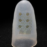 Recent advances in materials, fabrication strategies and device designs for flexible and stretchable electronics and sensors make it possible to envision a not-too-distant future where ultra-thin, flexible circuits based on inorganic semiconductors can be wrapped and attached to any imaginable surface, including body parts and even internal organs. Robotic technologies will also benefit as it becomes possible to fabricate 'electronic skin' that, for instance, could allow surgical robots to interact, in a soft contacting mode, with their surroundings through touch. Researchers have now demonstrated that they can integrate high-quality silicon and other semiconductor devices on thin, stretchable sheets, to make systems that not only match the mechanics of the epidermis, but which take the full three dimensional shapes of the fingertip - and, by extension, other appendages or even internal organs, such as the heart.
Aug 15th, 2012
 Doping, the process of adding impurity atoms to semiconductors to provide free carriers for conduction, has been pivotal to microelectronics since its early stages. In particular doping germanium at high concentrations to make it highly conductive is the subject of intense research, because it lies at the heart of novel developments in integrated silicon-compatible lasers and quantum information processing devices. Researchers have now demonstrated a method to densely pack dopant molecules on the germanium surface, which then self-organize to form molecular patterns with one phosphorus dopant atom every two germanium atoms. The key finding is that when you deposit phosphine molecules on a germanium surface, they naturally form molecular patterns with one phosphorus atom every two germanium atoms that densely pack the surface.
Aug 14th, 2012
 Subscribe to our Nanotechnology Spotlight feed