Showing Spotlights 169 - 176 of 262 in category All (newest first):
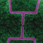
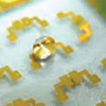 A single drop of water can be fatal to electrical circuits. To prevent water damage, current electronic devices are well sealed and packaged with polymer passivation. Researchers in Korea have now gone one step further and made water resistance a feature of the device itself by incorporating nonwetting, superhydrophobic components into the electronic device. They demonstrated this novel idea with a source/drain structure in a thin-film transistor. This work combines superhydorphobicity with electronic devices, especially resistive switching memory devices. Although much research has been done on either topic, few works report the combination of combining superhydrophobicity and electronic devices. This is a novel approach to combine two different concepts to get a synergic effects.
Oct 5th, 2011
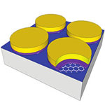 Electronic memory devices are increasingly expected to provide not only greater storage density, but also faster access to information. As storage density increases, however, power consumption and unwanted heat generation also increase, and the fidelity of accessing the memory is frequently diminished. Various platforms exist to overcome these hurdles and, increasingly, graphene finds it way into computer memory technology. The most recent example are experiments that demonstrate the benefits of graphene as a platform for flash memory which show the potential to exceed the performance of current flash memory technology by utilizing the intrinsic properties of graphene.
Sep 5th, 2011
 Electronic devices with muscles-like stretchability have long been pursued, but not achieved due to the requirement that all materials in the devices - electrodes, semiconductor, and dielectric - are stretchable. In their pursuit of fully flexible and stretchable electronic devices, researchers have already reported stretchable solar cells and transistors as well as stretchable active-matrix displays. The nanomaterials used for these purposes range from coiled nanowires to graphene. Recently, researchers at UCLA have successfully demonstrated a stretchable polymer composite that is highly transparent and highly conductive, and applied this nanocomposite material to fabricating stretchable devices. This work represents a proof-of-concept, highly stretchable semiconductor device wherein every part of the device is intrinsically stretchable.
Aug 22nd, 2011
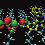 Using single molecules as electronic components like diodes, switches or transistors is the ultimate goal for future electronic nanotechnology devices. In order to explore the electronic properties of a single molecule, researchers have to make electrical contact between electrodes and molecules - and this has proven to be a big challenge. Though many efforts have been made to realize single-molecule electronics, it is still impossible to fabricate a practical single-molecule integrated circuit. One of the problems is the lack of viable methods for wiring each functional molecule. Researchers have now demonstrated a novel method for controlling single molecule chemical reactions - a kind of 'chemical soldering'.
Jul 28th, 2011
 There is a physical and electrical disconnect between the world of electronics and the world of biology. Electronics tend to be rigid, operate using electrons, and are inherently two-dimensional. The brain, as a basis for comparison, is soft, operates using ions, and is three-dimensional. Researchers have therefore been looking to find different routes to create biocompatible devices that work well in wet environments like biological systems. In an exiting new development, researchers from North Carolina State University have fabricated a memory device that is soft, entirely based on liquid-based matter, and functions well in wet environments - opening the door to a new generation of biocompatible electronic devices.
Jul 19th, 2011
 The field of single-molecule magnets is very promising, since an individual magnetic molecule represent the ultimate size limit to store and processing information. Magnetic molecules are considered very promising for spintronics since they can store a bit of information in an extremely small volume. However, in order to make magnetic molecules work, one has to find a way to measure their magnetization. Usual approaches are often very invasive and may lead to a strong perturbation of the properties of the molecules. A European research team has now designed and realized a novel hybrid spintronic nanodevice where the state of the molecule is measured 'indirectly', through a sensor coupled with the molecule.
Jul 5th, 2011
 One enabling technology for printed and flexible electronics devices is the use of a special silver nanoparticle ink that allow the patterning of silver microelectrodes by omnidirectional printing. Taking an important step towards enabling desktop manufacturing - or personal fabrication - using very low cost, ubiquitous printing tools, researchers have now demonstrated a pen-on-paper approach as a low-cost, portable fabrication route for printed electronic and optoelectronic devices. The team demonstrates the fabrication of electronic art, flexible displays, conductive text, and radio frequency antennas with their technique. The printed features can withstand repeated bending and folding while maintaining high conductivity.
Jun 27th, 2011
 Conventional metal patterning in the electronics industry is done by a photo-resist patterning with a photo-mask and metal evaporation in a vacuum chamber. This technology require expensive vacuum conditions, high processing temperatures, many steps, and toxic chemicals to fabricate one layer of a metal pattern. Furthermore, it is almost impossible to change the design of the expensive photomask once it is fabricated. Researchers have now developed a high-resolution metal nano-patterning technique by combining solution deposited metal nanoparticles and a femtosecond laser without using conventional vacuum deposition or photo-masks. With this method, the time and cost associated with high-resolution metal patterning can be reduced dramatically without using time-consuming vacuum processes and the pattern design can be easily changed in a digital manner without using expensive photo-masks.
Jun 22nd, 2011
 Subscribe to our Nanotechnology Spotlight feed