Showing Spotlights 65 - 72 of 338 in category All (newest first):
 This review summarizes the current industrial graphene synthetic and analytical methods, as well as recent academic advancements in larger-scale or sustainable synthesis of graphene. Specific emphasis is placed on recent research in the use of flash Joule heating as a rapid, efficient, and scalable method to produce graphene and other 2D nanomaterials. Challenges and opportunities in the larger-scale synthesis of graphene and a perspective on the broader use of flash Joule heating for larger-scale 2D materials synthesis are discussed.
Jan 19th, 2022
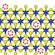
 Researchers developed a holistic approach, which predicts both Li-ion storage and supercapacitive properties and hence identifies various important electrode materials that are common to both devices, may pave the way for next-generation energy storage systems. By leveraging the big-data generated by the computational pipeline, the team trains crystal graph-based machine learning models and demonstrates how this data-driven model could be helpful for the rapid discovery of potential materials from other databases.
Jan 13th, 2022
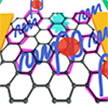 The use of graphene-based field-effect transistors is one of the most powerful biosensing units for the detection of numerous biological and biochemical analytes. In new work, researchers propose a microscopic model of mycotoxin detection via graphene-based aptasensors enabling improvement of biosensor sensitivity, which is based on the investigation of aptamer interaction mechanism with graphene channel during binding of targeted molecules. The limit of detection is estimated at only 1 pM and time response in just 10 seconds, making the developed platform a high-performance device.
Dec 22nd, 2021
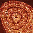 Many 2D materials with atomic-scale thicknesses suffer from oxidation and degradation effects under ambient conditions, which is one of the biggest obstacles in their practical applications. A 75-month study used atomic force microscopy to investigate the long-term evolution of oxidative defects on transition metal dichalcogenides (TMDs). Intriguingly, the researchers found that long-term storage in ambient conditions led to evolution of a distinct ring-like pattern resembling the tree-lines arising from seasonal changes.
Nov 22nd, 2021
 Precise patterning of 2D materials is a route to computation and storage using 2D materials, which can deliver potentially better performance and much lower power consumption compared to the technology of today. Researchers now demonstrate an etching process that makes it possible to downsize nanostructures to the 10-20 nm range and obtain smooth edges, sharp corners, and feature sizes significantly below the resolution limit of electron beam lithography. The nanostructured 2D materials can be used themselves or as etch masks to pattern other nanomaterials.
Sep 4th, 2021
 Negative differential resistance (NDR), which describes a decrease in electrical current as the applied bias increases, has always been one of the hottest topics in solid-state electronic devices since L. Esaki first demonstrated this phenomenon in heavily-doped Ge p-n junctions in 1958. Researchers now report the modulation of a unique room-temperature NDR effect with high peak current in ambipolar black phosphorus transistors. The simplicity of this structure, combined with the recent progress in scalable production of BP films, makes the BP NDR devices promising for practical electronic applications.
Aug 10th, 2021
 Photodetectors with blackbody response show significant applications in remote sensing and infrared imaging. However, up to now, few works have demonstrated excellent response to blackbody radiation (weak irregular radiation from a real object), which is essential to reliably evaluate their potential in practical detections. Researchers now have demonstrated van der Waals unipolar barrier photodetectors with nBn and pBp heterostructures. Designing unipolar barriers with conventional materials is challenging due to the strict requirements of lattice and band matching.
Jun 24th, 2021
 For the enormous promises of graphene and other two-dimensional (2D) materials to be fulfilled, scientists need a much better understanding of how specific types of defects in the crystal structure, including those that change location over time, affect its properties. To do that, they first need to identify the location and type of defect and then be able to precisely alter the structure of 2D materials in order to tailor their properties for applications based on them. Addressing this issue, researchers now have demonstrated structural engineering and atomic-scale analysis of graphene up to a level that so far has not been possible.
Jun 17th, 2021
 Subscribe to our Nanotechnology Spotlight feed