Showing Spotlights 73 - 80 of 330 in category All (newest first):
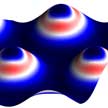 Periodically strained graphene harbors correlated electronic phases similar to those previously observed in magic angle twisted bilayer graphene. By precisely rotating two stacked sheets of graphene one can induce superconducting and insulating phases depending on the electric density. This behavior is extremely desirable because it significantly reduces energy losses in electronic devices making them more efficient and durable. Researchers have now proposed an alternative way to obtain similar phases. Their approach relies on periodically straining a graphene sheet rather than stacking layers on top of each other.
Aug 13th, 2020
 Charge density wave (CDW) is a quantum mechanical phenomenon, which induces distortion in the crystal structures of some low-dimensional (1D or 2D) metals, when the temperature is reduced. Such distorted crystal structure is known as CDW phase and its resistivity is much higher than the original symmetric phase. Since the switching between symmetric and CDW phase can also be made by the application of external electric field, these materials are technologically important and have attracted immense attention in the nanoelectronics community.
Aug 6th, 2020
 Borophene is the name for atomically thin, two-dimensional (2D) sheets of boron. Whereas boron is a nonmetallic semiconductor in its bulk form, it becomes a metallic conductor in 2D, even at a thickness of only one atomic layer. Among 2D materials, borophene has attracted considerable attention owing to its unique chemical structure and impressive electronic conductivity and surface properties. A recent review of the state of borophene research discusses various growth techniques and application areas for borophene and provides an in-depth summary of the material's electronic, optical, thermal, and elastic properties compared to its 2D cousins.
Jul 21st, 2020
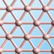
 The electronic and optical properties of 2D materials can be controlled by mechanical deformations of their crystal structure. This route to tailor the properties of materials is called strain engineering and it is a rapidly evolving field of research in nanomaterials. Straintronics, however, is somewhat hampered by technical issues related to the fast and reliable control of the applied strain. Researchers have now developed a versatile and straightforward platform to control the biaxial strain in atomically thin layers.
Jun 17th, 2020
 Superconducting materials, which entirely lose their electrical resistance at low temperatures, have become ever more widespread over recent years. Nevertheless, the fascinating phenomenon of superconductivity does not cease to surprise, as the kinds of materials able to superconduct, as well as the mechanisms through which superconductivity emerges, have become increasingly diverse. One of the prime examples is found in the compound 2D material tantalum disulfide, where the critical temperature below which superconductivity appears increases multifold as the crystal is made thinner down to a monolayer.
May 8th, 2020
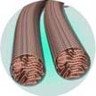 Deep brain stimulation (DBS) is an effective treatment for many neurological disorders, but despite its widespread utilization the underlying mechanisms and downstream effects of DBS remain poorly understood. One major issue to understand the therapeutic mechanism of DBS is to map the wide variety of brain responses at both the local and global levels. Researchers have developed a highly MRI-compatible graphene fiber electrode that enables full activation pattern mapping by functional magnetic resonance imaging under DBS without the occurence of artifacts resulting from magnetic field interference.
Apr 20th, 2020
 Researchers have developed black phosphorus (BP) functionalized graphene films, resulting in record toughness. The formation of covalent bonding between BP and graphene oxide (GO) nanosheets not only reduces the voids of GO film but also improves the alignment degree of GO nanosheets, resulting in high compactness of the GO film. After further chemical reduction and pi-pi stacking interactions by conjugated AD molecules, the alignment degree of reduced graphene oxide (rGO) nanosheets was further improved, and the voids in lamellar graphene film were also further reduced. The toughness of this graphene film reaches the highest value recorded to date.
Apr 9th, 2020
 Researchers report the direct writing of laser-induced graphene on a Kevlar textile. The transformation of Kevlar into graphene can be attributed to the photothermal effect induced by CO2 laser irradiation. Specifically, this resulted in high localized temperature, leading to the ablation and depolymerization of the Kevlar fiber. The remaining carbon atoms are recombined and 'recrystallized' into graphene. Based on this technique, it becomes feasible to prepare various types of flexible electronics on different commercial textiles such as silk and cotton. This will enable the efficient and customized preparation of multi-functional textile electronics.
Mar 11th, 2020
 Subscribe to our Nanotechnology Spotlight feed