Showing Spotlights 33 - 40 of 48 in category All (newest first):
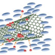 Their unique combinations of liquid and solid-like properties allow liquid crystals to be used pervasively in the electro-optical display technology - known as liquid crystal display (LCD). In new work, researchers have observed that a dilute suspension of a small amount of multi-walled carbon nanotubes in a nematic liquid crystal (in the nematic LC phase the molecules are oriented in parallel but not arranged in well-defined planes) results in a significantly faster nematic switching effect on application of an electric field.
Dec 13th, 2013
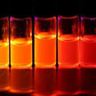 Quantum dots are expected to deliver lower cost, higher energy efficiency and greater wavelength control for a wide range of products, including lamps, displays and photovoltaics. Unfortunately, the toxicity of the elements used for efficient quantum dot based LEDs is a severe drawback for many applications. Therefore, light-emitting devices which are based on the non-toxic element silicon are extraordinary promising candidates for future QD-lighting applications. Researchers have now demonstrated highly efficient and widely color-tunable silicon light-emitting diodes (SiLEDs). The emission wavelength of the devices can easily be tuned from the deep red (680 nm) down to the orange/yellow (625 nm) spectral region by simply changing the size of the used size-separated silicon nanocrystals.
Feb 8th, 2013
 The size of pixels is one of the key limiting features in the state of the art of holographic displays systems. Holography is a technique that enables a light field to be recorded and later reconstructed when the original light field is no longer present, due to the absence of the original objects. The resolution and field of view in these holographic systems are dictated by the size of the pixel, i.e. the smallest light scattering element. To address the limitations of current holographic systems due to their pixel size, a research team set out to use nanostructures as the smallest possible light-scattering elements for producing holograms. They harnessed the extraordinary conductive and light scattering abilities of nanotubes and patterned an array of carbon nanotubes to produce a high resolution hologram.
Oct 1st, 2012
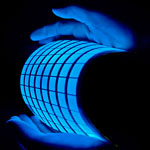
 Quantum dots, because they are both photoluminescent and electroluminescent and have unique physical properties, will be at the core of next-generation displays. Compared to organic luminescent materials used in organic light emitting diodes (OLEDs), QD-based materials have purer colors, longer lifetime, lower manufacturing cost, and lower power consumption. Another key advantage is that, because QDs can be deposited on virtually any substrate, you can expect printable and flexible displays of all sizes. To date, the integration of QDs into a full-color LED structure has not been possible due to the difficulty in patterning individual red-green-blue (RGB) QDs onto the pixelated display panel. Now, a Samsung team has demonstrated a novel transfer printing approach which enables fine patterning of high-quality QD films for large-area (4-inch diagonal), full-color displays mounted on glass as well as on flexible plastic substrates.
Feb 28th, 2011
 OLEDs - organic light-emitting diodes - are full of promise for a range of practical applications. OLED technology is based on the phenomenon that certain organic materials emit light when fed by an electric current and it is already used in small electronic device displays in mobile phones, MP3 players, digital cameras, and also some TV screens. With more efficient and cheaper OLED technologies it will possible to make ultra flat, very bright and power-saving OLED televisions, windows that could be used as light source at night, and large-scale organic solar cells. In contrast to regular LEDs, the emissive electroluminescent layer of an OLED consists of a thin-film of organic compounds. Exciton quenching and photon loss processes still limit OLED efficiency and brightness. Organic light-emitting transistors (OLETs) are alternative, planar light sources combining, in the same architecture, the switching mechanism of a thin-film transistor and an electroluminescent device. Thus, OLETs could open a new era in organic optoelectronics and serve as test beds to address general fundamental optoelectronic and photonic issues.
May 6th, 2010
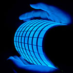
 With all the buzz that is being created by portable e-book readers, it's worth taking a look at one of the advanced display technologies - also often referred to as electronic paper - that make these devices happen. Unlike a conventional flat panel display, which uses a power-consuming backlight to illuminate its pixels, electronic paper reflects light like ordinary paper and is capable of holding text and images indefinitely without drawing electricity, while allowing the image to be changed later. Because they can be produced on thin, flexible substrates an due to their paper-like appearance, electrophoretic displays are considered prime examples of the electronic paper category. Electrophoretic displays already are in commercial use, for instance in the Kindle or in the Sony Reader, but so far the displays are mostly black and white. There are still cost and quality issues with color displays. New work by researchers in South Korea shows that organic ink nanoparticles could provide an improved electronic ink fabrication technology resulting in e-paper with high brightness, good contrast ratio, and lower manufacturing cost.
Jan 27th, 2010
 OLEDs - organic light-emitting diodes - are full of promise for a range of practical applications. With more efficient and cheaper OLED technologies it becomes possible to make ultraflat, very bright and power-saving OLED televisions, windows that could be used as light source at night, and large-scale organic solar cells. One of the drawbacks of this technology, apart from its currently high manufacturing cost, are problems with the OLED fabrication process where issues such as material damage, yield, and thickness uniformity haven't been completely solved yet. Researchers in Japan have now proposed a nanoparticle-based deposition method that might be able to overcome these fabrication problems.
Nov 23rd, 2009
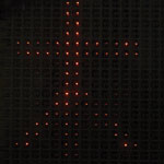 In a previous Nanowerk Spotlight we have reported about the work of Chinese scientists who demonstrated that a sheet of carbon nanotube (CNT) thin film could be a practical magnet-free loudspeaker simply by applying an audio frequency current through it . The team has now reported that their CNT films can also work as an incandescent display, driven by a simple addressing circuit with response times faster than that of liquid crystal displays (LCDs). At the same time, the incandescent light of the CNT film is almost nonpolarized, and will not have the viewing-angle problem of LCDs. The CNT films in vacuum can be heated to incandescence and cooled down in about 1 millisecond by turning on and shutting off the heating voltage.
May 22nd, 2009
 Subscribe to our Nanotechnology Spotlight feed