Showing Spotlights 17 - 24 of 48 in category All (newest first):
 New work describes how to control the kinetics of ion-capturing/ion-releasing regimes in liquid crystals by means of nanoparticles. Various types of nanomaterials and alignment layers are considered major components of the next generation of advanced liquid crystal devices. While the steady-state properties of ion-capturing/ion-releasing processes in liquid crystals doped with nanoparticles and sandwiched between alignment films are relatively well understood, the kinetics of these phenomena remains practically unexplored.
Feb 9th, 2018
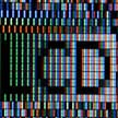
 For enhanced visualization experience, high resolution display technology with fast frame rate to suppress the motion blur at that resolution is essential. In modern display technologies, which are mostly active matrix display system, there are planar thin film transistors (TFTs) which enable both high resolution and fast imaging. Scaled TFTs can provide high resolution. Fast switching can be facilitated by the scaling as well as high mobility channel material. In new work, researchers have shown that both high resolution and fast frame rate display technology is possible, irrespective of the active channel material.
Nov 14th, 2017
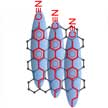 Image sticking phenomena in liquid crystal (LC) devices became obvious soon after the production of the first nematic LC displays and have been a concern ever since. Now, researchers have developed a method to reduce the presence of excess ionic impurities by using a graphene electrode in the LC cell. Graphene shows high optical transmittance and high electrical conductivity, and therefore, graphene can be used as transparent electrodes.
Oct 24th, 2017
 New work work shows the state of the art of engineering in wearable display technology. Researchers have demonstrated a passive matrix quantum dot light-emitting diode (QLED) display fully integrated with flexible electronics. They realized the visualization of meaningful information such as images, recorded healthcare data, and other messages using their display. This ultrathin and ultrasoft QLED array can be conformally laminated on human skin.
Aug 29th, 2017
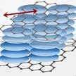 In conventional liquid crystal displays (LCD), the liquid crystal (LC) material is contained in conventional LC cells, where the polyimide layers are used to align the LC homogeneously in the cell, and the transmissive indium tin oxide (ITO) electrodes are used to apply the electric field to reorient the LC along the field. Now, researchers have experimentally demonstrated that monolayer graphene films on the two glass substrates can function concurrently as the LC alignment layers and the transparent electrodes to fabricate an LC cell, without using the conventional polyimide and ITO substrates.
Jul 11th, 2017
 Many of the electronic devices we use in our daily life rely on liquid crystal display (LCD) technologies. LCDs get their name from the special liquid crystal solution that is contained between two thin glass plates inside the display. An electric field applied across the liquid crystal layer changes optical properties of the liquid crystals thus enabling their use in displays. A new paper reports several interesting size effects including monotonous and non-monotonous dependence of the total concentration of mobile ions in liquid crystals on the thickness of the cell and/or on the concentration of nanoparticles.
Jun 30th, 2017
 An recent analysis of the combined effect of nanoparticles and substrates on the concentration of mobile ions in liquid crystals considers both 100% pure and contaminated with ions substrates and nanoparticles. The results could be very useful for engineers trying to apply nanotechnology to liquid crystal devices. Specifically, the control of mobile ions in liquid crystals by means of nanoparticles and substrates of the cell tailored for specific applications - liquid crystal displays, light shutters, switches, modulators, etc.
Mar 8th, 2017
 Liquid crystals used in modern devices such as laptops, tablets and smartphones typically contain a small fraction of ionic contaminants. These ion contaminants can originate from multiple sources during the chemical synthesis of materials, in the process of assembling the device, and in its daily use.
In the case of LCDs, mobile ions in liquid crystals lead to such undesirable effects as image sticking, image flickering, and slow response. A promising solution to reduce the concentration of mobile ions in liquid crystal devices can be found by merging liquid crystals and nanotechnology.
Liquid crystals used in modern devices such as laptops, tablets and smartphones typically contain a small fraction of ionic contaminants. These ion contaminants can originate from multiple sources during the chemical synthesis of materials, in the process of assembling the device, and in its daily use.
In the case of LCDs, mobile ions in liquid crystals lead to such undesirable effects as image sticking, image flickering, and slow response. A promising solution to reduce the concentration of mobile ions in liquid crystal devices can be found by merging liquid crystals and nanotechnology.
Jan 23rd, 2017
 Subscribe to our Nanotechnology Spotlight feed