Showing Spotlights 2505 - 2512 of 2838 in category All (newest first):
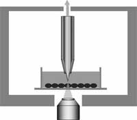
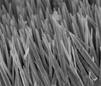 Large-scale and high-density semiconductor arrays with one-dimensional ("1D" - where one dimension of the structure is nanoscale) nanostructures have been extensively studied for their potential application in future electrooptical devices. Among them, zinc oxide (ZnO) is considered to be very attractive for high-efficiency short-wavelength optoelectronic nanodevices because of its large exciton binding energy of 60 meV and high mechanical and thermal stabilities. ZnO nanorod/ nanowire arrays have also been demonstrated to be highly versatile and proven to be quite effective in piezoelectric nanogenerators, dye-sensitized solar cells, photonic crystals, superhydrophobic surfaces, and even biodevices due to their biocompatibility. One of the issues researchers are still grappling with is the synthesis of ZnO nanowire arrays. On one hand, high-temperature techniques such as chemical vapor deposition (CVD) have been widely employed and result in high quality nanostructures. However, these methods are energy-consuming and expensive. On the other hand, there are several advantages of growing semiconducting nanostructures directly on conducting metal substrates, for instance the formation of robust electrical contacts during the growth. Such wet chemical methods, which are appealing for their low temperature, facile manipulation, and potential for scale-up have recently been developed for the production of aligned ZnO nanostructures and so far the most successful route has been seeded growth on ZnO-nanoparticle-coated substrates. In these two-step processes the coating of the substrate for the formation of a nucleation layer remains complex and difficult/irreproducible. Therefore, large-scale, low-cost controllable growth of well-aligned ZnO 1D nanostructures on properly fitting substrates via a one-step synthetic approach is still crucially needed for novel applications to become practicable. Researchers in China now have demonstrated exactly such a highly effective solution by growing well-aligned ZnO 1D nanostructures on various inert metal substrates at low temperature on a large scale.
Jun 18th, 2007
 Just because something is really small doesn't mean it has to do with nanotechnology.
Jun 15th, 2007
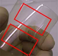
 Thin, flexible displays have become an everyday component in many electronic gadgets from cell phones to digital cameras and MP3 players. Most of these displays are based on LCD technology, liquid crystals combined with polymeric structures, and one of their drawbacks is that their manufacturing cost grows rapidly with increasing screen size. A recently developed alternative approach for thin, flexible displays makes use of thermochromic composite thin-films. Thermo- chromism is the ability of a substance to change color due to a change in temperature. This first of a kind thermochromic display is based on films with thermochromic nanoparticles and embedded conductive wiring patterns. Based on the ease of fabrication and simple architecture, thermochromic displays could have advantages in lowering the display unit cost and, due to their heating pulse control scheme, can also lower power consumption compared with conventional displays.
Jun 14th, 2007
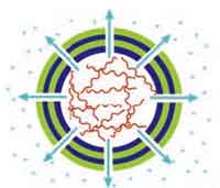 You cut yourself in the finger - and a few days later your skin has completely healed again. Biological organisms have an amazing ability to automatically initiate self-healing and self-repair when they sustain damage. Materials engineers are dreaming about making materials that could do the same thing. Imagine self-repairing cars, planes, bridges or buildings. These materials could be of particular use in structures that are at present impractical or impossible to repair, such as electronic circuit boards, implanted medical devices or spacecraft. Self-repairing materials would have a massive impact on virtually all industries, lengthening product lifetimes, increasing safety, and lowering product costs by reducing maintenance requirements. Thanks to nanotechnology, these visions are coming closer to reality. One approach is the use of nanocontainers that possess the ability to release encapsulated active materials in a controlled way, leading to a new family of self-repairing coatings.
Jun 13th, 2007
 Thin-film transistors (TFTs) and associated circuits are of great interest for applications including displays, large-area electronics and printed electronics (e.g. radio-frequency identification tags - RFID). Well-established TFT technologies such as amorphous silicon and poly-silicon are well-suited for many current applications - almost all mobile phone color screens use them - but face challenges in extensions to flexible and transparent applications. In addition, these TFTs have modest carrier mobilities, a measure of the velocity of electrons within the material at a given electric field. The modest mobility corresponds to a modest operating speed for this class of TFTs. Organic TFTs are generally better suited for flexible applications, and can be made transparent. However, mobilities in organic TFTs are generally quite low, restricting the speed of operation and requiring relatively large device sizes. Researchers at Purdue University, Northwestern University, and the University of Southern California now have reported nanowire TFTs that have significantly higher mobilities than other TFT technologies and therefore offer the potential to operate at much higher speeds. Alternatively, they can be fabricated using much smaller device sizes, which allows higher levels of integration within a given chip area. They also provide compatibility with a variety of substrates, as well as the potential for room-temperature processing, which would allow integration of the devices with a number of other technologies (e.g. for displays).
Jun 12th, 2007
 Cells are the smallest 'brick' in life's building structures. Every living organism is made of cells. Individual cells carry their own DNA and have their own life cycle. Considering that larger organisms, such as humans, are basically huge, organized cell cooperatives, the study of individual live cells is a hugely important scientific task. Among the most significant technical challenges for performing successful live-cell imaging experiments is to maintain the cells in a healthy state and functioning normally on the microscope stage while being illuminated. Especially if scientists want to look into cellular processes that occur in cells in their natural state and that cannot be observed by traditional cytological methods. It is well known that cells move, grow, duplicate, and move from point A to point B. Up to now people studied these mechanical properties with optical microscopes because it is the most common and simple method, very efficient, a very well developed and advanced technology. However, with optical microscopes detection is limited to objects no smaller than the wavelengths of the visible region of light, roughly between 400 and 700 nanometers. Distances or movement smaller than this range cannot be seen with these instruments. Researchers in Kyoto, Japan have applied a near-field optical approach to measure cell mechanics and were able to show intriguing data of nanoscale cell membrane dynamics associated with different phenomena of the cell's life, such as cell cycle and cell death.
Jun 11th, 2007
 Ethanol is all the rage these days. Although we have been drinking ethanol, an alcohol, for thousands of years (fermented beverages such as beer and wine may contain up to 15-25% ethanol by volume), the recent interest has been sparked by its use as a renewable fuel alternative to gasoline. Indeed, the largest single use of ethanol is as a motor fuel and fuel additive. Ethanol is produced by fermentation when certain species of yeast metabolize sugar. The process works with all biological feedstocks that contain appreciable amounts of sugar or materials that can be converted into sugar such as starch or cellulose. The primary feedstock for ethanol production in the U.S. is corn. In Brazil, the world's leading ethanol producer, it's mostly derived from sugar cane. While there is a heated controversy over the economic and ecological benefits of using biomass for producing ethanol fuel, it seems that nanotechnology's jack-of-all-trades, the carbon nanotube (CNT), might provide a solution here as well. CNTs are increasingly recognized as promising materials for catalysis, either as catalysts themselves, as catalyst additives or as catalyst supports. Researchers in China now have used CNTs loaded with rhodium (Rh) nanoparticles as reactors to convert a gas mixture of carbon monoxide and hydrogen into ethanol. This appears to be the first example where the activity and selectivity of a metal-catalyzed gas-phase reaction benefits significantly from proceeding inside a nanosized CNT reaction vessel.
Jun 8th, 2007
 OLEDs - organic light-emitting diodes - are full of promise for a range of practical applications not too far into the future. Today, OLEDs are used in small electronic device displays in mobile phones, MP3 players, digital cameras, etc. With more efficient and cheaper OLED technologies we soon will see ultraflat, very bright and power-saving OLED televisions, windows that could be used as light source at night, and large-scale organic solar cells. In contrast to regular LEDs, the emissive electroluminescent layer of an OLED consists of a thin-film of organic compounds. What makes OLEDs so attractive is that they do not require a backlight to function. Thus they draw far less power and, when powered from a battery, can operate longer on the same charge. OLED devices can be made thinner and lighter than comparable LED devices. Last but not least, OLEDs can be printed onto almost any substrate with inkjet printer technology, making new applications like displays embedded in clothes or roll-up displays possible. Unfortunately there are also drawbacks to this technology. Apart from its currently high manufacturing cost, the major problem is device degradation and the limited lifetime of organic materials. In particular, the most commonly used material for the anode, ITO (indium tin oxide), is a less than optimal material for future high-performance OLEDs. New research indicates that nanoimprinted semitransparent metal electrodes, replacing ITO electrodes, are an attractive and potentially practical solution for OLEDs and other organic devices.
Jun 7th, 2007
 Subscribe to our Nanotechnology Spotlight feed