Showing Spotlights 2489 - 2496 of 2838 in category All (newest first):
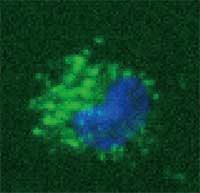 A quantum dot (QD), also called a nanocrystal, is a semiconductor nanostructure that can be as small as 2 to 10 nm. The usefulness of quantum dots comes from their peak emission frequency's extreme sensitivity - quantum mechanical in nature - to both the dot's size and composition. QDs have been touted as possible replacements for organic dyes in the imaging of biological systems, due to their excellent fluorescent properties, good chemical stability, broad excitation ranges and high photobleaching thresholds. However, the main drawback of QDs is their toxicity and therefore their application is problematic. If this toxicity problem could be addressed, QDs may one day be safely utilized in many areas. For instance, cadmium telluride (CdTe - which is toxic) QD based nanocomposites can be used as fluorescent probes for biological imaging, they can also be utilized to monitor targeted drug delivery and for controlled modification of structural and functional properties of intracellular components. Scientists in Ireland have been using gelatin during the production of CdTe QDs thereby reducing the toxicity of the particles. Their approach could be useful for the development of other nanoparticle composites with low toxicity as well.
Jul 13th, 2007
 Our modern lifestyle exposes us to hundreds of chemical substances every day, quite a number of them are known to be hazardous, if not outright toxic. The long, long list ranges from toxic chemicals and heavy metals included in electronic waste to insecticides and herbicides that find their way into the food chain, to flame retardant chemicals in buildings and furniture. A European project has set out to give an overview of already used and conceivable applications of nanotechnology in order to replace hazardous chemicals. The overall idea behind this project is to identify new nanotechnology applications which could help to reduce the risks related to hazardous substances and chemical processes. Currently, nanotechnologies are not contributing exceptionally to an increase in the substitution of hazardous substances for safer ones. However, experts believe that this could well change in the future. These are two of the messages coming out of a study by STOA, the European Parliament's Scientific Technology Options Assessment committee, on the role of nanotechnology in chemical substitution.
Jul 12th, 2007
 Curing cancer is on of the many promises of nanotechnology. Although scientists have been making amazing progress in this area, there are still significant challenges that need to be overcome before highly selective, targeted anti-cancer therapy becomes available for everyday clinical use. A nanotechnology-based system to eradicate cancer needs four elements: 1) Molecular imaging at the cellular level so that even the slightest overexpressions can be monitored; 2) effective molecular targeting after identifying specific surface or nucleic acid markers; 3) a technique to kill the cells, that are identified as cancerous based on molecular imaging, simultaneously by photodynamic therapy or drug delivery and 4) a post molecular imaging technique to monitor the therapeutic efficacy. One of the problems today is that these four techniques are used separately or ineffectively, resulting in an overall poor therapeutic outcome. In what could amount to a quantum leap in cancer nanotechnology, researchers have now integrated these techniques simultaneously in vitro and shown that this results in higher therapeutic efficacies for destroying cancer cells. Their demonstration of multi-component molecular targeting of surface receptors and subsequent photo-thermal destruction of cancer cells using single-walled carbon nanotubes (SWCNTs) could lead to a new class of molecular delivery and cancer therapeutic systems.
Jul 11th, 2007
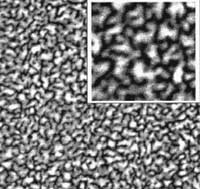 An incredible amount of research has gone, and still goes, into the understanding of the properties of nanoscale particles. In order to capitalize on that research, scientists and engineers have to take the next step, which is to turn nanoparticle laboratory results into usable materials and devices. One way to use engineered nanoparticles in the real world is in thin films. Nanoparticulate thin films are thin layers, sometimes only a few nanometers thick, of composite materials that contain nanoparticles. These new materials have a wide range of applications such as nanoelectronics, magnetic storage devices, or optical coating. However, most processes used to fabricate thin nanocomposite films with high nanoparticle fillings suffer from random nanoparticle agglomeration causing formation of irregularly shaped nanostructured features within the composite. Unfortunately, the improved mechanical, tribological and electrical properties of the nanocomposites over the host matrix materials (mostly polymers) are only attainable if the nanoparticle inclusions are of uniform size and shape with very good degree of dispersion. A newly developed technique now allows a wide range of control of including metal nanoparticle into polymer matrices in a single step process.
Jul 10th, 2007
 New technology, whether it is a novel cancer treatment or an innovative approach to farming, almost always comes with risk. Those risks are often first - and most severely - felt by industry workers, and nanotechnology is no different. Today, workers around the world are exposed to nanoparticles on a daily basis. There is much speculation, yet so far, little definitive information about how exposure affects workers. A report released by the International Council on Nanotechnology in November 2006, offers a clear picture of the situation. "The properties for which novel nanoscale materials are designed may generate new risks to workers, consumers, the public, and the environment. While some of these risks can be anticipated from experiences with other synthetic chemicals and with existing knowledge of ambient and manufactured fine particles, novel risks associated with new properties cannot easily be anticipated based on existing data." Questions, such as how to measure toxicity and how to monitor and control exposure, remain unanswered.
Jul 9th, 2007
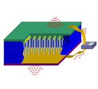 For the over 100 million people worldwide who suffer from diabetes, testing blood glucose is the only way to be sure that it is within normal range and allows them to adjust the insulin dose if it is not. The current method for monitoring blood glucose requires poking your finger to obtain a blood sample. The equipment needed to perform the blood test includes a needle device for drawing blood, a blood glucose meter, single-use test strips, and a log book. Now imagine this scenario: your doctor implants a tiny device the size of a rice grain under your skin. This device automatically and accurately measures your blood glucose levels at whatever intervals, even constantly if required. It transmits the data to an external transceiver. If any abnormality is detected, the device warns you and automatically transmits the data to your doctor's computer. This scenario is one of the many promises of nanomedicine where in-situ, real-time and implantable biosensing, biomedical monitoring and biodetection will become an everyday fact of normal healthcare. Nanosensors are already under intense development in laboratories around the world. One of the important components for implantable nanosensors is an independent power source, either a nanobattery or a nanogenerator that harvests energy from its environment, so that the sensor can operate autonomously. Not only has such a nanogenerator now been developed, but a new prototype has been demonstrated to effectively generate electricity inside biofluid, e.g. blood. This is an important step towards self-powered nanosystems.
Jul 6th, 2007
 If you have seen the movie The Matrix then you are familiar with 'jacking in' - a brain-machine neural interface that connects a human brain to a computer network. For the time being, this is still a sci-fi scenario, but don't think that researchers are not heavily working on it. What is already reality today is something called neuroprosthetics, an area of neuroscience that uses artificial microdevices to replace the function of impaired nervous systems or sensory organs. Different biomedical devices implanted in the central nervous system, so-called neural interfaces, already have been developed to control motor disorders or to translate willful brain processes into specific actions by the control of external devices. These implants could help increase the independence of people with disabilities by allowing them to control various devices with their thoughts (not surprisingly, the other candidate for early adoption of this technology is the military). The potential of nanotechnology application in neuroscience is widely accepted. Especially single-walled carbon nanotubes (SWCNT) have received great attention because of their unique physical and chemical features, which allow the development of devices with outstanding electrical properties. In a crucial step towards a new generation of future neuroprosthetic devices, a group of European scientists developed a SWCNT/neuron hybrid system and demonstrated that carbon nanotubes can directly stimulate brain circuit activity.
Jul 5th, 2007
 Continuing miniaturization has moved the semiconductor industry into the nano realm with leading chip manufacturers well on their way to CPUs using 32nm process technology (expected by 2009). There are some real challenges ahead for chip designers, particularly in moving deeper and deeper into the nanoscale, where at some point in the near future they will reach physical limits of the traditional logic MOSFET (metal-oxide-semiconductor field-effect transistor) structure. In addition to physical barriers, semiconductor companies will also reach economic barriers where profitability will be squeezed hard in view of the exorbitant costs of building the necessary manufacturing capabilities if present day technologies are extrapolated. Quantum and coherence effects, high electric fields creating avalanche dielectric breakdowns, heat dissipation problems in closely packed structures and the relevance of single atom defects are all roadblocks along the current road of miniaturization. Enter nanoelectronics (note that microelectronics, even if the gate size of the transistor is below 100 nm, is not an implementation of nanoelectronics, as no new qualitative physical property related to reduction in size are being exploited). Its goal is to process, transmit and store information by taking advantage of properties of matter that are distinctly different from macroscopic properties. Understanding nanoscale transport and being able to model and simulate nanodevices requires an entirely new generation of simulation tools and techniques.
Jul 3rd, 2007
 Subscribe to our Nanotechnology Spotlight feed