Showing Spotlights 2401 - 2408 of 2838 in category All (newest first):
 We have written Spotlight after Spotlight pointing out the numerous challenges that researchers are facing with regard to nanofabrication. Uncountable research papers have been written about the numerous methods available for synthesizing nanomaterials. What today is called 'nanofabrication' deals with the issues of fabricating complex and functional nano- and microstructures by integrating these synthesized nanomaterials. To complicate matters, many of these nanomaterials are fragile, either because they are composed of a limited number of atomic layers or because they are 'soft', i.e., of biological or molecular nature. This fragile nature of some materials creates a major headache: how to integrate them at an individual level into devices without altering their structure and, consequently, their properties during device fabrication. Currently, researchers use mainly e-beam lithography and, in some cases, focused ion beam to fabricate devices which incorporate nanostructures. These methods have been proven to be very useful, for example for investigations of carbon nanotubes. However, they can not be applied on fragile nanostructures, because they damage or contaminate the structures - this could result from exposure to high energy particle beams; the requirement for lift-off steps; exposure to chemicals, etc. Researchers have now shown that individual nanostructures can be integrated into functional devices using dynamic nanostenceling which allows the integration of individual nanostructures into devices using entirely scanning probe based methods and without exposure to damaging conditions, such as high-energy charged particles, heat, or resists.
Nov 19th, 2007
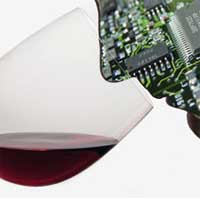 The concept of e-noses - electronic devices which mimic the olfactory systems of mammals and insects - is very intriguing to researchers involved in building better, cheaper and smaller sensor devices. A better understanding of the reception, signal transduction and odor recognition mechanisms for mammals, combined with achievements in material science, microelectronics and computer science has led to significant advances in this area. Nevertheless, the olfactory system of even the simplest insects is so complex that it is still impossible to reproduce it at the current level of technology. For example, the biological receptors are regularly replaced during the life of mammals in a very reliable way so that the receptor array does not require to be recalibrated. The performance of existing artificial electronic nose devices is much more dependent on the sensor's aging and, especially, the sensor's replacement and frequently require a recalibration to account for change. Moreover, current electronic nose devices based on metal oxide semiconductors or conducting polymers that specifically identify gaseous odorants are typically large and expensive and thus not adequate for use in micro- or nano-arrays that could mimic the performance of the natural olfactory system. Nanotechnology is seen as a key in advancing e-nose devices to a level that will match the olfactory systems developed by nature. Nanowire chemiresistors are seen as critical elements in the future miniaturization of e-noses. It is now also believed that single crystal nanowires are most stable sensing elements what will result in extending of life-time of sensors and therefore the recalibration cycle. Last year we reported on a research effort Towards The Nanoscopic Electronic Nose. Scientists involved in this effort now report a second-generation, far more advanced e-nose system based on metal oxide nanowires.
Nov 16th, 2007
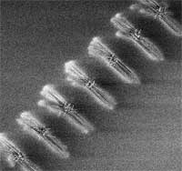
 A team of researchers have come up with an inexpensive way of making complex networks of carbon nanotubes that can be stamped onto circuit boards. They were able to create an inexpensive and relatively simple method for creating these predefined networks. The scientists arranged silicon pillars in the shape of the network they wanted and then coated the top of the pillars with silicon dioxide. The suspended single-walled carbon nanotubes adhered to the tops of pillars, growing taut and straight. A Raman spectroscopy (RS) laser not only assigned specific properties to each individual nanotube, it was also capable of destroying any unwanted nanotubes.
Nov 15th, 2007
 Slowly but surely the realization begins to sink in that there is no quick buck to be made for individual investors in nanotechnology companies (except for the people pushing investment advice of course). Existing public nanotechnology firms as a group have performed sub-standard (to put it politely); there isn't exactly a flood of nanotech IPOs on the horizon; and many product advances that have to do with nanotechnologies are made by large companies which either make these advances silently (witness the cosmetics industry) or tout them as major breakthroughs (like IBM's 'airgap' technology). In any case, all these nanotechnology-based materials are incremental improvements over existing materials - leading to better coatings, more efficient batteries and fuel cells, better performing materials, etc. - and not revolutionary devices. Of course, when we look back 10 years from now, there will have been one or two great performing nanotech stocks (I will tell you in 2017 who they are); but then there will be one or two great performing stocks in almost any other investment sector. Nevertheless, there are many start-ups and early stage companies out there - some might even make it to the IPO (initial public offering) stage or be bought by larger companies - and given the nature of the field, with its broad and multidisciplinary character, it certainly is helpful for the professional investor to be able to gauge the nanotechnology investment landscape from a technology perspective. A recent article describes a methodology to categorize different nanotechnologies into one of three types: passive, active, or hybrid nanotechnologies, each with different time horizons for expected commercial viability.
Nov 14th, 2007
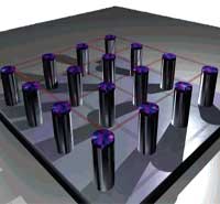
 Fundamental nanotechnology research in laboratories advances rapidly, as witnessed by the hundreds of new research papers that get published every month. The big bottleneck in getting these new technologies from the lab translated into commercial products is the lack of suitable large-scale fabrication techniques. Almost all laboratory experiments involve elaborate set-ups and are quite tricky processes that require a lot of skill and expertise on part of the researchers. To a large degree, nanotechnology today is more an art than a basis for industrial technologies. Think about a 15th century monk spending 10 years painstakingly writing and painting a single bible - that's where nanotechnology is today; but where we need to get to is something that resembles modern high speed printing machines where you print thousands of books an hour. Take for instance nanowires. Researchers have used nanowires to create transistors like those used in memory devices and prototype sensors for gases or biomolecules. A common approach in the lab is to grow nanowires like blades of grass on a suitable substrate, mow them off and mix them in a fluid to transfer them to a test surface, using some method to give them a preferred orientation. When the carrier fluid dries, the nanowires are left behind like tumbled jackstraws. Using scanning probe microscopy or similar tools, researchers hunt around for a convenient, isolated nanowire to work on, or place electrical contacts without knowing the exact positions of the nanowires. It's not a technique suitable for mass production. However, researchers have now developed a technique that allows them to selectively grow nanowires on sapphire wafers in specific positions and orientations accurately enough to attach contacts and layer other circuit elements, all with conventional lithography techniques. This fabrication method requires a minimum number of steps and is compatible with today's microelectronics industry.
Nov 13th, 2007
 Some pundits writing about nanotechnology get carried away by their own hype and talk about self-assembly as if bottom-up fabrication technologies, where molecules get assembled into everyday products, are just around the corner. We took a swing at this in our Spotlight from a few days ago (Nanotechnology 'pencil sharpeners' add to researchers' nanofabrication toolbox). Today we bring you another example from the cold reality of the labs that makes clear how early stages this whole field of self-assembly really is. Today, when researchers - with both feet firmly on the ground - talk about self-assembly they mostly talk about template-assisted nanocrystal superlattices in the form of planar thin films. Bottomline is that even the controllable fabrication of highly ordered homogeneous nanostructures on surfaces remains a difficult challenge. And IBM's much touted 'self-assembling nanotechnology' (see: IBM applies self-assembling nanotechnology to conventional chip manufacturing) is nothing more than a patterning process that creates a film with trillions of holes around the on-chip wiring. Moving from a planar geometry of self-assembled nanoscale building blocks such as nanocrystals or nanotubes to a free-standing, three-dimensional multifunctional architecture is not a trivial undertaking. Researchers are just about to make the first steps to such multifunctional (still nanoscale) hierarchical architectures that both retain the properties of the nanocrystals and offer multifunctionality.
Nov 12th, 2007
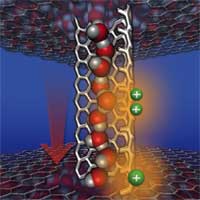 Nanofluidic channels, confining and transporting tiny amounts of fluid, are the pipelines that make the cellular activities of organisms possible. Nanoscale channels carry nutrients into cells and waste from cells and they also transport water into and out of the cell. Body temperature, digestion, reproduction, fluid pressure in the eye, and water conservation in the kidney are only a few of the processes in humans that depend on the proper functioning of cellular water channels. Special proteins called aquaporins can transport water through the cell membrane at a high rate while effectively blocking everything else - even individual protons, the nuclei of hydrogen atoms. The aquaporin channels are so narrow that no molecule larger than water can pass through, effectively forcing them through like beads on a chain. A unique distribution of amino acid residues along the pore wall also accounts for the channel's ability to move water quickly. To keep out molecules smaller than water there is also a chemical filter, formed by the specific orientation and distribution of the amino acid residues lining the pore. Thus water, and only water, flows freely through the aquaporin nanochannels, the direction of flow depending only on changing relative pressure inside and outside the cell. This intriguing mechanism has attracted the attention of nanotechnology researchers who see it as a blueprint for the construction of nanoscale water pumps. A molecular dynamics simulation conducted by Chinese researchers proposes a design for such a molecular pump constructed with a carbon nanotube.
Nov 9th, 2007
 Titanium oxide - due to its versatile optical, electrical and photochemical properties, its relative abundance and low cost, and its non-toxicity - is an important ceramic material with numerous applications as pigments; powders for catalytic or photocatalytic applications; colloids and thin films for photovoltaic, electrochromic, photochromic, electroluminescence devices and sensors; components for antireflecting coatings; or porous membranes for ultrafiltration. Nanocrystalline titania has become a prominent material for dye-sensitized solar cells (DSSCs, also known as 'Grätzel cells' after their inventor), which are photoelectrochemical cells that use photo-sensitization of wide-band-gap mesoporous oxide semiconductors. One major problem with the use of titania in solar cells is that its bandgap does not match that of visible light and titania therefore can only absorb 3-4% of the energy from sunlight. Grätzel cells decrease the bandgap of titania by using dye-absorbed TiO2 nanocrystals as one of the electrodes, resulting in a higher solar energy conversion of 10% or more. Other methods use doping and indeed the application of nitrogen-doped titania as photocatalyst has received increasing attention over the last years because N-doping is found to be particularly effective in decreasing the bandgap of anatase (many of the properties of titania depend on the structure of the TiO2 phase - mainly anatase, brookite and rutile). In order for photocatalysis-based applications to become commercially viable, it will be critical to design low-cost, reproducible, synthetic methods that yield controlled, reproducible, and easy-to-handle nanomaterials processed as coatings with high surface area and high porosity. Researchers in France and Spain now describe for the first time nanostructured coatings that fulfill all these requirements.
Nov 8th, 2007
 Subscribe to our Nanotechnology Spotlight feed