Showing Spotlights 2393 - 2400 of 2838 in category All (newest first):
 An important property of polyaniline (PANi), a polymer, is its electric conductivity. This makes it suitable for the manufacture of electrically conducting fibers. Consequently, PANi and other conductive polymers have been extensively studied for optical and electronic applications and many practical syntheses of one-dimensional (1D) nanostructured PANi have already been developed. However, preparation of water-soluble, conductive PANi nanowires with controllable morphologies and sizes, especially with good processibility, is still a big challenge. A possible solution could lie in the use of self-assembled proteins, such as plant viruses, as nanotemplates for the synthesis of these nanowires. For instance, genetically modified viruses have already been proposed as templates for the assembly of nanometer-scale components of electronic circuits. Researchers now have successfully demonstrated the fabrication of water-dispersible, conductive PANi nanowires using the rod-like tobacco mosaic virus (TMV) as a template. They have also shown that much longer conductive PANi/TMV nanowires (greater than the length of a native TMV particle) can be formed by a hierarchical assembly process.
Nov 30th, 2007
 Governments always struggle when faced with regulating highly complex subject matters such as nanotechnologies. Primarily concerned with managing the potential risks to the environment, human health and the safety of workers (EHS), regulators often feel overwhelmed by the complexity and novelty of new technologies, stymied by a lack of data, and confused by conflicting research findings and advice from various interest groups. In the meantime, against a backdrop of a legal environment that ranges from gaping holes to regulatory vacuum, research organizations and early-adopting industry players push ahead with the new technology. Not being able to create any breathing room for lengthy political and legal considerations, the last 15-20 years have seen several governments adopting voluntary environmental programs (VEPs), arguing that this is the only viable proportional option for the time being. It is estimated that there are some 300 VEPs in the European Union and over 200 in the United States, dealing with matters such as climate change, energy, waste, water, toxic materials, agriculture, manufacturing, mining, forestry, hotels, hospitals, and financial institutions. If these voluntary programs work is subject to debate - some apparently do, some less so. In the case of manufactured nanomaterials, the risk properties remain largely unknown and it is unclear what exactly should be regulated. For the VEPs that are in place for nanomaterials, governments are urging companies to submit health and safety information on the nanomaterials they produce or commercialize. In order to investigate whether voluntary government programs will be sufficient to ensure the safety of manufactured nanomaterials, researchers have analyzed a sampling of voluntary programs in the fields of environmental health and safety in the United States over the past 20 years, with a view towards their applicability in the case of manufactured nanomaterials
Nov 29th, 2007
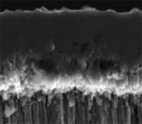 In most mechanical systems, friction or vibration are often considered to be negative attributes because they results in wear and unnecessary energy dissipation. Tribological issues such as friction, wear, and vibration have always plagued developers of small-scale mechanical devices. As devices get smaller and even reach the nanoscale, this problem becomes more acute due to the extreme surface-to-volume ratios these devices have. In nanomachines damage to even a single atom layer could mean disaster. Nanotechnology researchers basically have two ways to address this problem: they either could apply traditional tribological methods by trying to integrate dampers and low-friction materials with their nano- and microdevices - which becomes increasingly complex and costly at the nanoscale - or they could try and develop intrinsic damping materials that have hard, low-fiction surfaces to lower wear yet still maintain high compressibility and elastic properties to provide resistance to vibrations and shocks. Finding materials that address these problems individually is not difficult but fabricating a structure that combines all of them is nearly impossible because of the conflicting nature of these attributes. However, in what researchers have dubbed a 'nanomattress', a unique structure containing aligned carbon nanotubes (CNTs) covered with a hard layer of diamond-like carbon (DLC) results in a carbon-based composite material with outstanding mechanical properties.
Nov 28th, 2007
 In October, Sony introduced the world's first OLED (organic light-emitting diode) television set. This The 11-inch OLED TV - although quite expensive at $1,700 - realizes an astonishing 3mm-thinness (at thinnest point) and unparalleled image quality. What makes OLEDs so attractive is that they do not require a backlight to function and therefore they draw far less power and, when powered from a battery, can operate longer on the same charge. OLED devices can be made thinner and lighter than comparable LED devices. Another major leap forward compared to current display technologies is that OLEDs can be printed onto almost any substrate with inkjet printer technology, making new applications like displays embedded in clothes or roll-up displays possible. Unfortunately there are also drawbacks to this technology, in particular its currently high manufacturing cost. A possible solution could lie in cost efficient mass production methods using printing or spraying techniques. These methods use semiconductor materials that are processed in the form of a dispersion, comprising soluble conjugated polymers or precursor molecules as well as colloidal, organic or inorganic nanoparticles. Inkjet-printing represents a powerful, economic tool for accurate deposition of liquids which is not only useful for graphics applications, but has also enormous potential for the direct writing of electronic devices. Researchers in Austria have now shown for the first time the highly reproducible ink-jet printing of semiconducting nanocrystals for the fabrication of optoelectronic devices.
Nov 27th, 2007
 The benefits of new technologies, whether they are new medical treatments, an innovative approach to farming or new ways of generating energy, almost always come with some new risks as well. In the emerging stages of a new technology, experts and the public generally differ in their perceptions of risk. While this might be due to social and demographic factors, it is generally assumed by scientists who conduct risk research that experts' risk assessments are based more strongly on actual or perceived knowledge about a technology than lay people's risk assessments. Nevertheless, whether the risks are real or not, the public perception of an emerging technology will have a major influence on the acceptance of this technology and its commercial success. If the public perception turns negative, potentially beneficial technologies will be severely constrained as is the case for instance with gene technology. It is not surprising that a new study found that, in general, nanoscientists are more optimistic than the public about the potential benefits of nanotechnology. What is surprising though, is that, for some issues related to the environmental and long-term health impacts of nanotechnology, nanoscientists seem to be significantly more concerned than the public.
Nov 26th, 2007
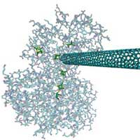 Just because hydrogen is a clean fuel doesn't mean that hydrogen production is a clean process. As more and more companies and investors jump onto the 'cleantech' bandwagon, hydrogen occupies an important place in this vision of a sustainable, carbon-free, and non-polluting energy future. If you look closer though, you'll find that you are not always told the full story about "clean" hydrogen. The U.S. department of Energy's Hydrogen Energy Roadmap foresees up to 90% of hydrogen production coming from fossil fuels - coal, gas, oil. In other words, a clean fuel is produced by the same dirty fuel that is causing all the problems we are facing today (read more in our recent Spotlight: Nanotechnology could clean up the hydrogen car's dirty little secret). Hydrogen can be produced in a clean way, of course, but the greatest challenge to clean hydrogen production is cost - so far, the cheapest way today to produce hydrogen is from fossil fuels. And as long as the political will and the resulting large-scale funding isn't there, this won't change. Unfortunately, large-scale deployment of artificial water-splitting technologies looks unlikely given the need for large amounts of expensive precious metals - such as platinum, which currently cost about $45,000 per kilogram, and which will become scarce at some point in the future - required to catalyze the multi electron water-splitting reactions. Intriguingly, there are mechanism of biological hydrogen activation found in nature and researchers have identified several microbes that can activate the dihydrogen bond through the catalytic activity of hydrogenases (enzymes that play a vital role in anaerobic metabolism). Scientists hope that these proteins could one day serve as catalysts for hydrogen production and oxidation in fuel cells. So far, their efforts have been hampered by the difficulty of incorporating these enzymes into electrical devices because the enzymes do not form good electrical connections with fuel cell components. New research now demonstrates the first successful electrical connection between a carbon nanotube and hydrogenase.
Nov 23rd, 2007
 Earlier this year, the Science Policy Council of the U.S. Environmental Protection EPA (EPA) issued the final version of its Nanotechnology White Paper. The purpose of this White Paper is to inform EPA management of the science issues and needs associated with nanotechnology, to support related EPA program office needs, and to communicate these nanotechnology science issues to stakeholders and the public. While this has been the publicly most visible EPA activity with regard to nanotechnology, it is less widely known that the EPA, since 2002, has been spending more than $25 million through its Science to Achieve Results (STAR) grants program for 86 projects on research into the environmental aspects of nanotechnology. The projects are broadly grouped into two main categories: 1) nanotechnology applications - examining beneficial uses - where the areas of research include green manufacturing, contamination remediation, sensors for environmental pollutants, and waste treatment; and 2) nanotechnology implications - examining the potentially adverse health effects to humans and the environment - where research is grouped into five categories: aerosol, exposure assessment, fate and transport, life-cycle analysis, and toxicity.
Nov 21st, 2007
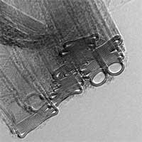 Tie a rock to the end of a piece of ribbon, then spin it over your head. It will be pulled taut as the rock circles about. Now, imagine a ribbon 62,000 miles long, anchored near the equator with a weight on the other end. The centrifugal force of the earth's rotation will make it behave the same way. You'll end up with not only the world's biggest nunchuck, but also a kind of elevator to outer space. A space elevator is one of those ideas from 1950s-style futurism that are so whacky they might just work. The single most difficult task in building the Space Elevator is achieving the required tether strength-to-weight ratio - in other words, developing a material that is both strong enough and light enough to support the 60,000 mile long tether. This material has become available in the form of carbon nanotubes (CNTs). The challenge ahead is to weave these raw CNTs into a useful form - a space worthy climbable ribbon. Assembling carbon nanotubes into commercially usable fibers is still one of the many challenges that nanotechnology researchers are faced with when trying to exploit the amazing properties of many nanomaterials. Apart from ambitious large-scale projects like the space elevator, CNT-based fibers will have many applications, from protective fabrics and coatings in military applications, higher performance materials for sports equipment to transparent conductive films and, eventually, as a replacement for copper wire in transmitting electrical power and signals. Researchers in the UK are making good progress in developing scalable fabrication techniques for high performance CNT fibers.
Nov 20th, 2007
 Subscribe to our Nanotechnology Spotlight feed