Showing Spotlights 2297 - 2304 of 2839 in category All (newest first):
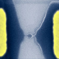
 Future nanomanufacturing processes will rely on two basic principles: a combination of chemical synthesis and self-assembly on one hand and robotic nanofabrication on the other. While the former is a controlled 'natural' process relying on chemistry and self-organization principles of nature, the latter will be an industrial process similar in concept to today's automated manufacturing assembly lines. Robotic assembly lines in modern factories have come a long way since the early 20th century when Henry Ford first used an assembly line on an industrial scale for his Model T automobile. Nevertheless, the principle is the same. Rather than having a single craftsman or team of craftsmen create each part of a product individually and assemble them together into a single item, an assembly line is a (often completely automated) manufacturing process in which interchangeable parts are added to a product in a sequential manner to create a finished product. While sporadic automation of certain tasks has already begun (for instance, automated microrobotic injection of foreign materials into biological cells), nanotechnology techniques today are pretty much where the industrial world was before Ford's assembly line - a domain of highly skilled artisans and not of automated mass production. It has long been a dream for nanotechnologists that robots could one day be used in an assembly line type of process to manufacture nanodevices. Researchers are beginning to develop the first rudimentary nanomanipulation devices that could lead to future automated manufacturing systems. Now, a team of scientists in Canada have reported the first demonstration of closed-loop force-controlled grasping at the nanonewton level.
Apr 25th, 2008
 Following up on yesterday's Spotlight about graphene quantum dots, today we look at what might be the first realistic application of this revolutionary material. Back in December we reported on the development of transparent and conductive graphene-based composites for use as window electrodes in solid-state dye sensitized solar cells. While the researchers who conducted this work produced graphene by chemical oxidation of graphite, a multi-step process, new results from the University of Manchester group that discovered graphene in 2004 show a simpler route to producing graphene films that cannot only be used for solar cells but might be well suited for liquid crystal displays.
Apr 24th, 2008
 We have written about scientists' fascination with graphene - the flat one-atom thick sheet of carbon - before. Over the past couple of years, graphene has become a new model system for condensed-matter physics - the branch of physics that deals with the physical properties of solid materials - because it enables table-top experimental tests of quantum relativistic phenomena, some of which are unobservable in high-energy physics. The behavior of electrons in graphene is very different from their behavior in typical semiconductors. In the latter, they possess a mass, and a finite energy (called the energy gap) is necessary to move the electrons from the valence to the conductance band and they move like regular particles, increasing their speed as they get accelerated. In graphene, electrons move with a constant speed - much faster than electrons in other semiconductors - independent of their kinetic energy (similar to the behavior of photons), and there is no energy gap. Graphene, which basically is an unrolled, planar form of a carbon nanotube therefore has become an extremely interesting candidate material for nanoscale electronics. Researchers in the UK have now, for the first time, shown that it is possible to carve out nanoscale transistors from a single graphene crystal.
Apr 23rd, 2008
 The toxicity issues surrounding carbon nanotubes (CNTs) are highly relevant for two reasons: Firstly, as more and more products containing CNTs come to market, there is a chance that free CNTs get released during their life cycles, most likely during production or disposal, and find their way through the environment into the body. Secondly, and much more pertinent with regard to potential health risks, is the use of CNTs in biological and medical settings. CNTs interesting structural, chemical, electrical, and optical properties are explored by numerous research groups around the world with the goal of drastically improving performance and efficacy of biological detection, imaging, and therapy applications. In many of these envisaged applications, CNTs would be deliberately injected or implanted in the body. For instance, CNT-based intercellular molecular delivery vehicles have been developed for intracellular gene and drug delivery in vitro. What these CNTs do once inside the body and after they discharge their medical payloads is not well understood. Cell culture studies have shown evidence of cytotoxicity and oxidative stress induced by single-walled carbon nanotubes (SWCNTs), depending on whether and to what degree they are functionalized or oxidized. A new study at Stanford University tested non-covalently pegylated SWCNTs as a 'least toxic scenario', and oxidized, covalently functionalized nanotubes as a 'most toxic scenario' in a study on mice. It was found that SWCNTs injected intravenously into nude mice do not appear to have any significant toxicity during an observation period of four months following injection.
Apr 22nd, 2008
 Safe, efficient and compact hydrogen storage is a major challenge in order to realize hydrogen powered transport. According to the U.S. Department of Energy's Freedom CAR program roadmap, the on-board hydrogen storage system should provide a gravimetric density of 6 wt% at room temperature to be considered for technological implementation. Currently, the storage of hydrogen in the absorbed form is considered as the most appropriate way to solve this problem. Research groups worldwide are seeking and experimenting with materials capable of absorbing and releasing large quantities of hydrogen easily, reliably, and safely. One candidate material that is being considered as a candidate for hydrogen storage media is single-walled carbon nanotubes. So far, carbon nanotubes have been unable to meet the DOE's hydrogen storage target. New theoretical work from China suggests that silicon nanotubes can store hydrogen more efficiently than their carbon nanotube counterparts. This raises the possibility that, after powering the micro-electronics revolution, silicon could also become a key material for the future hydrogen economy.
Apr 21st, 2008
 Following just two days after we wrote about the food industry's deafening silence on their nanotechnology research and development, the Investor Environmental Health Network today released a report that demonstrates that sectors affected by product toxicity risks are doing a poor job of informing shareholders of market risks they face due to toxic chemicals in their products. The report specifically addresses the situation for companies dealing with nanomaterials by noting that manufacturers are not disclosing the evidence of health risks of nanotechnology products, nor the lack of adequate product testing prior to their sales. An interesting observation is that some nanomaterial manufacturers are more open to communicating potential uncertainties than their customers. These customers of the nanomaterials are the manufacturers of an array of products from electronics to food and cosmetics - and they tend not to disclose the potential health and financial risks. IEHN's conclusion is that investors should be apprised of the state of the science by a company, instead of being misled to believe that the serious questions have been answered.
Apr 18th, 2008
 The European Union currently spends about 740 million Euros (roughly $1.2 billion) annually in public funding on nanotechnology research. This is almost on par with the U.S. National Nanotechnology Initiative (NNI) budget of $1.28 billion (2007). Almost 40% of public EU nanotechnology funding takes place in Germany and it is estimated that about half of the European companies active in nanotechnology are based in Germany, making the country the clear nanotechnology leader in Europe. Germany's strengths include a well structured research and development infrastructure and a high level of research in the various subfields of nanotechnology. The industrial base for utilizing the results of this research is also in place. About 700 companies are currently involved in the development, application, and sales and marketing of nanotechnological products. What sets public nanotechnology policy in Germany and other European countries apart from the U.S. is a more deliberate attempt to create, and evolve over time, an integrated approach in the development of nanotechnology research, trying to link sustainability questions and technology development.
Apr 17th, 2008
 The food industry is excited about the potential of nanotechnology. Food companies are very much involved in exploring and implementing nanotechnology applications in food processing, packaging and even growing - but you don't hear about it anymore. At least not from the companies. Large industrial food companies, no stranger to big and expensive media campaigns, have buried the subject of nanotechnology in their public relations graveyard. Take Kraft Foods for example. While it took the industry's nanotechnology lead when it established the Nanotek Consortium in 2000, it has since pulled back completely on the PR front. The Nanotek Consortium even was renamed the 'Interdisciplinary Network of Emerging Science and Technologies' (INEST), is now sponsored by Altria, and its single webpage makes no mention of food at all. Doing our regular check on the websites of large food companies we again found not a single reference to 'nanotechnology' or even 'nano'. The same is true for large food industry associations such as the Grocery Manufacturers/Food Products Association (GMA/FPA), which represents the world's leading food, beverage and consumer products companies. Faced with a complete nanotechnology communications blackout from the manufacturers, it is left to activist groups like Friends of the Earth to frame the discussion. These groups are trying to figure out what the food industry is up to and if there might be any risks involved that we should know about.
Apr 16th, 2008
 Subscribe to our Nanotechnology Spotlight feed