Showing Spotlights 329 - 336 of 336 in category All (newest first):
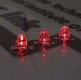 Ink-jet printing of metal nanoparticles for conductive metal patterns has attracted great interest as an alternative to expensive fabrication techniques like vapor deposition. The bulk of the research in this area focuses on printing metal nanoparticle suspensions for metallization. For example, silver and gold nanoparticle suspensions have been inkjet printed to build active microelectromechanical systems (MEMS), flexible conductors and radio frequency identification (RFID) tags. Nobel metals like silver and gold are preferred nanoparticles for ink-jet formulations because they are good electrical conductors and they do not cause oxidation problems. However, gold and silver still are too expensive for most high volume, ultra low-cost applications such as RFID tags with required unit costs below one cent. A new technique developed in Switzerland uses flame spray synthesis in combination with a simple in-situ functionalization step to synthesize graphene coated copper nanoparticles which are air-stable and can be easily handled at ambient conditions. This work illustrates graphene's potential as a protective shell material for nanoparticles, enabling control and design of the chemical reactivity of non-noble metals.
Oct 14th, 2008
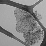 Carbon nanomaterials have been extensively used in electroanalysis, and the most common forms are spherical fullerenes, cylindrical nanotubes, and carbon fibers and blacks. Since the discovery that individual carbon nanotubes (CNTs) can be used as nanoscale transistors, researchers have recognized their outstanding potential for electronic detection of biomolecules in solution, possibly down to single-molecule sensitivity. To detect biologically derived electronic signals, CNTs are often functionalized with linkers such as proteins and peptides to interface with soluble biologically relevant targets. Now, for the first time, scientists have tested nanometal decorated graphene (actually graphite nanoplatelets, a thickness of 10 nm would contain approximately 30 graphene sheets, considering an interlayer spacing of 0.335 nm) in biosensor application. As it turned out, this novel biosensor is among the best reported to date in both sensing performance and production cost.
Sep 8th, 2008
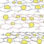 The electrical properties of graphene have been the topic of recent interest from various disciplines because this novel carbon material offers exciting opportunities to develop nanocomposites with unusual electronic catalytic properties. Most of these studies involve mechanical peeling of individual graphene sheets - one at a time - from a block of graphite. The requirement to obtain graphene as individual sheets and to maintain it in the reduced form introduces a certain level of complexity into the process of designing composite systems where, for instance, semiconductor or metal nanoparticle are anchored on graphene sheets. Without some form of intervention, the strong van der Waals interactions between reduced graphene sheets would cause them to collapse and aggregate. Researchers have now developed a simple photocatalytic method to anchor semiconductor nanoparticles on a single sheet of graphene using a solution-based process.
Jul 15th, 2008
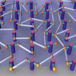 Since its discovery in 2004, graphene has created quite a buzz among scientists. The reason they are so excited is that two-dimensional crystals (it's called 2D because it extends in only two dimensions - length and width; as the material is only one atom thick, the third dimension, height, is considered to be zero) open up a whole new class of materials with novel electronic, optical and mechanical properties. For instance, the ultimate size limit for a nano-electromechanical system would be a nanoscale resonator that is only one atom thick, but this puts severe constraints on the material; as a single layer of atoms, it should be robust, stiff, and stable. Graphene, the simplest of the 2D conjugated carbon nanomaterials, could fit that bill. One hurdle for researchers is that current methods for the synthesis of two-dimensional, carbon-rich networks have many limitations including lack of molecular-level control and poor diversity. In a step to overcome these obstacles, researchers have now developed new synthetic strategies for forming monolayer films of conjugated carbon, in various configurations ranging from flat 2D sheets, to balloons, tubes and pleated sheets.
Jun 3rd, 2008
 Following up on yesterday's Spotlight about graphene quantum dots, today we look at what might be the first realistic application of this revolutionary material. Back in December we reported on the development of transparent and conductive graphene-based composites for use as window electrodes in solid-state dye sensitized solar cells. While the researchers who conducted this work produced graphene by chemical oxidation of graphite, a multi-step process, new results from the University of Manchester group that discovered graphene in 2004 show a simpler route to producing graphene films that cannot only be used for solar cells but might be well suited for liquid crystal displays.
Apr 24th, 2008
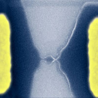 We have written about scientists' fascination with graphene - the flat one-atom thick sheet of carbon - before. Over the past couple of years, graphene has become a new model system for condensed-matter physics - the branch of physics that deals with the physical properties of solid materials - because it enables table-top experimental tests of quantum relativistic phenomena, some of which are unobservable in high-energy physics. The behavior of electrons in graphene is very different from their behavior in typical semiconductors. In the latter, they possess a mass, and a finite energy (called the energy gap) is necessary to move the electrons from the valence to the conductance band and they move like regular particles, increasing their speed as they get accelerated. In graphene, electrons move with a constant speed - much faster than electrons in other semiconductors - independent of their kinetic energy (similar to the behavior of photons), and there is no energy gap. Graphene, which basically is an unrolled, planar form of a carbon nanotube therefore has become an extremely interesting candidate material for nanoscale electronics. Researchers in the UK have now, for the first time, shown that it is possible to carve out nanoscale transistors from a single graphene crystal.
Apr 23rd, 2008
 There has been quite a buzz about graphene, a single atomic layer thick, plane of carbon atoms arranged in a honeycomb lattice. Discovered only in 2004, graphene exhibits many exotic properties and currently is considered the most exciting new material system among nanotechnology researchers. This rising star in material science exhibits remarkable electronic properties that qualify it for applications in future optoelectronic devices. In a first experimental study of the thermal conductivity of single-layer graphene, researchers found that on top of many unique electronic properties, graphene also is an extraordinary good heat conductor. Measurements revealed that graphene's near room temperature thermal conductivity, which is in the range from 3500-5300 W/mK, is much higher than that of diamond, the best bulk crystal heat conductor. It appears that the thermal conductivity of graphene is larger than conventionally accepted experimental values reported for individual suspended carbon nanotubes (CNTs) and corresponds to the upper bound of the highest values reported for single-wall CNT bundles. The superb thermal conduction property of graphene is beneficial for its proposed electronic applications and establishes graphene as an excellent material for thermal management also in optoelectronics, photonics and bioengineering.
Feb 21st, 2008
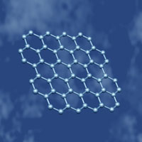
 Carbon comes in many different forms, from the graphite found in pencils to the world's most expensive diamonds. In 1980, we knew of only three basic forms of carbon, namely diamond, graphite, and amorphous carbon. Then, fullerenes and carbon nanotubes were discovered and all of a sudden that was where nanotechnology researchers wanted to be. Recently, though, there has been quite a buzz about graphene. Discovered only in 2004, graphene is a flat one-atom thick sheet of carbon. Existing forms of carbon basically consist of sheets of graphene, either bonded on top of each other to form a solid material like the graphite in your pencil, or rolled up into carbon nanotubes (think of a single-walled carbon nanotube as a graphene cylinder) or folded into fullerenes. Physicists had long considered a free-standing form of planar graphene impossible; the conventional wisdom was that such a sheet always would roll up. Initially using such high-tech gadgets like pencils and sticky tape to strip chunks of graphite down to layers just one atom thick, the process has now been refined to involve more expensive instruments such as electron beam and atomic force microscopes. Despite being isolated only three years ago, graphene has already appeared in hundreds of papers. The reason scientists are so excited is that two-dimensional crystals (it's called 2D because it extends in only two dimensions - length and width; as the material is only one atom thick, the third dimension, height, is considered to be zero) open up a whole new class of materials with novel electronic, optical and mechanical properties.
Aug 8th, 2007
 Subscribe to our Nanotechnology Spotlight feed