Showing Spotlights 313 - 320 of 338 in category All (newest first):
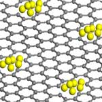
 Current protein detection approaches are mainly dominated by heterogeneous immunological (or separation) assay methods. These assays are usually low-throughput and frequently require multiple steps including multiple incubation and careful washing of a surface onto which the labeled reagent has bound. In contrast, homogenous immunoassays can overcome these problems. In these assays, the signal is affected by binding and can often be run without a separation step. Such assays can frequently be carried out simply by mixing the reagents and sample and making a physical measurement. Researchers in China and Japan have now developed a graphene oxide based fluorescence assay for fast, ultra-sensitive, and selective detection of protein and demonstrated its use for detection of a prognostic indicator in early-stage cancer, cyclin A2.
Sep 13th, 2010
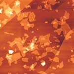
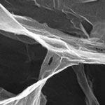 Given the massive interest and rapid developments in graphene research, scientists are now convinced that the controlled preparation of graphene-based materials with hierarchical and well-defined structures will pave the way for achieving high-performance applications of graphene in various technological fields such as optoelectronics, energy storage, polymer composites and catalysis. Self-assembly techniques have become some of the most effective strategies for this purpose. Although 2D self-assembly of graphene has been studied extensively from the perspectives of fundamental research and commercial applications, 3D self-assembly of 2D nanoscale graphene into functional macrostructures with well-defined networks remains as a great challenge and represents an important hurdle towards practical applications. Researchers in China have now provided a solution to this problem by demonstrating the successful preparation of self-assembled graphene hydrogel via a one-step hydrothermal process.
Jul 7th, 2010
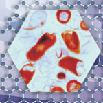 Researchers have made the surprising finding that graphene-based nanomaterials possess excellent antibacterial properties. Although antibacterial materials are widely used in daily life, and the antibacterial properties of nanomaterials are increasingly being explored and developed as commercial products, their cytotoxicity and biocompatibility has raised questions and concerns. Chinese researchers now found that graphene derivatives - graphene oxide, graphene oxide and reduced graphene oxide - can effectively inhibit bacterial growth. This is a significant finding as previous have proven that graphene, particularly graphene oxide, is biocompatible and cells can grow well on graphene substrates. Furthermore, while silver and silver nanoparticles have been well know to be antibacterial, they and other nanomaterials are often cytotoxic.
Jul 5th, 2010
 Before the superior electronic properties of graphene can be utilized in industrial products, researchers must find a way that allows the mass production of graphene-based devices. New work by a European research team now demonstrates the feasibility of graphene synthesis on commercially available cubic SiC/Si substrates of 300 mm and greater in diameter, which result in graphene flakes electronically decoupled from the substrate. This work demonstrates that it is possible to grow high-quality graphene layers on beta-SiC(001), i.e. on the cubic modification of this material. This is a very important step, since beta-SiC is commercially available and it can be well integrated into present electronic production processes.
Jun 18th, 2010
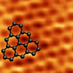
 Among the various production methods for carbon nanotubes and graphene, currently only chemical vapor deposition techniques demonstrate a significant opportunity for mass production of CNT material. Using the CVD process, which is based on the catalytic action of metals, manufacturers can combine a metal catalyst such as iron with reaction gases such as hydrogen to form carbon nanotubes inside a high-temperature furnace. In order to optimize the synthesis process, a detailed understanding of the interaction between nanotubes or graphene and metal atoms is required - something that has been missing so far. Researchers in France have now shown that it is possible to create atomic-scale defects in carbon nanotubes and in graphene in preselected positions with a focused electron beam and to use these defects as trapping centers for foreign atoms.
May 31st, 2010
 Graphite oxide sheet, now being named graphene oxide - a compound of carbon, oxygen, and hydrogen obtained by treating graphite with strong oxidizers - has attracted substantial interest as a possible intermediate for the manufacture of graphene. It has been largely viewed as hydrophilic - having a strong affinity for water illustrated by its excellent colloidal stability in water. In what should help to better understand and improve the solution processing of graphite oxide-based graphene materials and open up opportunities to design new functional graphite oxide-based hybrid materials, researchers have now reported that graphite oxide is amphiphilic - possessing both hydrophilic and lipophilic (fat-liking) properties - and can adsorb onto air-water, oil-water and solid-water interfaces.
May 26th, 2010
 As it is becoming clearer that one of the critical issues for developing functional nanomachines is the generation of energy required to power them, research into developing nanoscale energy sources has been picking up substantially. The energy to be fed into a nanogenerator is likely to be mechanical energy that is converted into electric energy that then will be used to power nanodevices without using a battery. With the emergence of nanotechnology and the use of nanomaterials, the field of piezoelectrics and nanopiezotronics has experienced a lot of new and interesting research efforts. Researchers in Korea have now demonstrated the first use of chemical vapor deposition-grown large-scale graphene sheets as transparent electrodes for fully transparent and flexible nanogenerators.
Apr 19th, 2010
 Silicon has dominated solid-state electronics for more than four decades but now a variety of other materials are being explored in photonic devices to expand the wavelength range of operation and to improve performance. Graphene is such a material - although most research on graphene so far has focused mainly on electronics. IBM researchers have now shown that graphene-based devices can be used in optical communications. Introducing this new material system into photonics could have a significant impact on mainstream optical applications. By using graphene, researchers make use of the internal electric field that exists at the interface of graphene and metal. Through a sophisticated combination of palladium and titanium electrodes they created a photodetector that does not rely on external current.
Apr 7th, 2010
 Subscribe to our Nanotechnology Spotlight feed