Showing Spotlights 321 - 328 of 336 in category All (newest first):
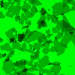 Graphene based sheets such as pristine graphene, graphene oxide, or reduced graphene oxide are basically single atomic layers of carbon network. They are the world's thinnest materials. A general visualization method that allows quick observation of these sheets would be highly desirable as it can greatly facilitate sample evaluation and manipulation, and provide immediate feedback to improve synthesis and processing strategies. Current imaging techniques for observing graphene based sheets include atomic force microscopy, transmission electron microscopy, scanning electron microscopy and optical microscopy. Some of these techniques are rather low-throughput. And all the current techniques require the use of special types of substrates. This greatly limits the capability to study these materials. Researchers from Northwestern University have now reported a new method, namely fluorescence quenching microscopy, for visualizing graphene-based sheets.
Dec 14th, 2009
 Chip structures already have reached nanoscale dimensions but as they continue to shrink below the 20 nanometer mark, ever more complex challenges arise and scaling appears not to be economically feasible any more. And below 10 nm, the fundamental physical limits of CMOS technology will be reached.
One promising material that could enable the chip industry to move beyond the current CMOS technology is graphene, a monolayer sheet of carbon. Notwithstanding the intense research interest, large scale production of single layer graphene remains a significant challenge. Researchers at Cornell University have now reported a new technique for producing large scale single layer graphene sheets and fabricating transistor arrays with uniform electrical properties directly on the device substrate.
Chip structures already have reached nanoscale dimensions but as they continue to shrink below the 20 nanometer mark, ever more complex challenges arise and scaling appears not to be economically feasible any more. And below 10 nm, the fundamental physical limits of CMOS technology will be reached.
One promising material that could enable the chip industry to move beyond the current CMOS technology is graphene, a monolayer sheet of carbon. Notwithstanding the intense research interest, large scale production of single layer graphene remains a significant challenge. Researchers at Cornell University have now reported a new technique for producing large scale single layer graphene sheets and fabricating transistor arrays with uniform electrical properties directly on the device substrate.
Dec 2nd, 2009
 Graphene is an impressive condensed matter system that, to all appearances, never ceases to impress and challenge our entrenched intuitions regarding solid state systems. But graphene is a highly atypical electronic system in that it consists of nothing but a surface. Researchers at Boston University have found that local deformations in a graphene sheet can strongly influence electron flow across the system, causing suppression of conductance at low densities, and making electrons behave as if they were living in a nanoribbon or quantum dot. All this without cutting the graphene sheet, which opens the prospect towards a reversible and controllable transport gap in monolayer graphene via strain engineering.
Oct 6th, 2009
 Nanostructures present novel material properties and interesting insight into new physical phenomena. However, from a technical and commercial application point of view, a successful bridging between the nanoscale specific significance with large-scale applications must be made to obtain these benefits. One of the 'hottest' nanomaterials at the moment is graphene, a one-atom thick sheet of carbon. Ribbons made from graphene, basically stripes that look like molecular chicken wire, show even more unconventional properties than graphene, especially when they are less than 100 nm wide. Any material approach to use graphene nanoribbons for larger-scale applications must be able to assemble them into macroscopic materials, while preserving their physical significance and novel properties at these larger scales. Researchers at MIT have addressed this issue by proposing hierarchical assemblies of graphene nanoribbons through hydrogen bonds, inspired by biological structures found in nature such as proteins and DNA macromolecules.
Oct 2nd, 2009
 The most promising applications of graphene are in electronics, detectors, and thermal management. The first graphene field-effect transistors have already been demonstrated. At the same time, for any transistor to be useful for analog communication or digital applications, the level of the electronic low-frequency noise has to be decreased to an acceptable level. Low frequency electronic noise dominates the noise spectrum to a frequency of about 100 kHz. Despite the fact that modern electronic devices such as cell phones and radars operate at a much higher carrier frequency, the low frequency noise is extremely important. Due to unavoidable non-linearities in devices and systems, the low frequency noise gets up-converted, and contributes to the phase noise of the system, thus limiting its performance. It is not possible to build a communication system or detector based on graphene devices until the noise spectral density is decreased to the level comparable with the conventional state-of-the-art transistors. Researchers at the University of California - Riverside have now reported the results of experimental investigation of the low-frequency noise in a double-gate graphene transistors.
Jul 14th, 2009
 Graphene has two distinct types of edges produced when it is cut - armchair type or zigzag type - which correspond to the two crystal axis of graphene. These edge types are predicted theoretically to have distinct electronic, magnetic, and chemical properties, but current fabrication methods have no way of controlling which type of edge is produced and are dominated by disorder. For example, a common method is to use plasma etching which is an isotropic etching process and is not selective in which crystallographic direction it etches. This is a problem in especially nanoelectronics applications and devices where the potential performance of the device depends strongly on the edge structure as well. A solution to this problem has now been found. Researchers have demonstrated anisotropic etching in single-layer graphene which produces connected graphene nanostructures with crystallographically oriented edges. This opens many future avenues to study graphene nanostructures such as nanoribbons, nanoconstrictions, and quantum dots with crystallographic edges.
Jun 30th, 2009
 Graphene is a recently discovered allotrope of carbon, which consists of a planar single sheet of carbon atoms arranged in honeycomb lattice. It has attracted tremendous attention of the nanotechnology research community owing to a number of unique physical properties. From a practical point of view, some of the most interesting characteristics of graphene are its extraordinarily high room temperature carrier mobility and recently measured extremely high thermal conductivity. The outstanding current and heat conduction properties of graphene are beneficial for the proposed electronic, interconnect, and thermal management applications. There is a realistic possibility that soon the fastest transistors and most sensitive detectors will be made out of graphene. For instance, we have just reported that next generation computer memory could be made of graphene. In order to build useful devices from materials which have only atomic thickness, one has to use extensively scanning electron microscopy, transmission electron microscopy, and focused ion beam processing. Unfortunately, all material characterization techniques which involve electron beam irradiation of the samples may result in damage to the material and disordering of the crystalline lattice. So far, despite the practical importance of the issue, the scale of this potential damage to single-layer of bi-layer graphene has not been investigated. What happens with the crystalline lattice has also been unclear.
Dec 30th, 2008
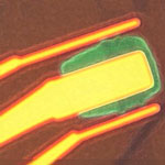
 Experiments with graphene have revealed some fascinating phenomena that excite researchers who are working towards molecular electronics. It was found that graphene remains capable of conducting electricity even at the limit of nominally zero carrier concentration because the electrons don't seem to slow down or localize. This means that graphene never stops conducting. Taking advantage of the conducting properties of graphene, researchers now have described how graphene memory could potentially be used as a new type of memory that could significantly exceed the performance of current state-of-the-art flash memory technology. Their results show the possibility to build next-generation memory devices with vast amounts of memory using nanocables with a silicon dioxide core and a shell of stacked sheets of graphene.
Nov 25th, 2008
 Subscribe to our Nanotechnology Spotlight feed