Showing Spotlights 305 - 312 of 336 in category All (newest first):
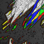
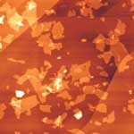
 In the decades-old quest to build artificial muscles, many materials have been investigated with regard to their suitability for actuator application (the ability of a material to reversibly change dimensions under the influence of various stimuli). Recently, hope in obtaining improved artificial muscles was revitalized by the discovery of the extraordinary mechanical and electrical properties of graphene and its chemical derivatives. A new study shows that electrical heating of graphene oxide nanoribbons mats results in reversible generation of 1.6% stress and maximum work capacity of about 40 J/kg, which is similar to that of natural muscle. Unlike previous studies, the team obtained the graphene material by chemical unzipping of multi-walled carbon nanotubes.
Mar 24th, 2011
 An important consideration for practical graphene applications is the fact that the physical characteristics of graphene are strongly dependent on the number of atomic planes, i.e. the properties of few-layer graphene are different from those of single layer graphene. Unfortunately, the one-atom thickness of graphene and its optical transparency make graphene identification and counting the number of atomic planes in few-layer graphene extremely challenging. This complicates the development of industrial-scale applications that would require the handling of large wafers with graphene. Current techniques for counting the number of atomic planes in few-layer graphene samples are either destructive, too complicated, or too slow. Researchers at UC Riverside have now developed a large-scale graphene recognition and quality control technique for industrial applications.
Feb 7th, 2011
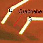
 Graphene is a very interesting nanomaterial with potential for applications in many different fields including nanoelectronics. However, the properties of graphene can vary broadly and depend sensitively on its integration in device structures and the details of its interaction with other materials, such as underlying substrates or gate dielectrics. Unlike other semiconductor electronic devices, where the active layer is buried below the surface and where microscopic details of transport cannot be directly examined, graphene is exposed at a surface and can be directly examined on the atomic scale using scanning tunneling microscopy (STM) and scanning tunneling spectroscopy (STS). New work now provides microscopic details of graphene interaction with a substrate in the most common device structure used so far.
Jan 27th, 2011
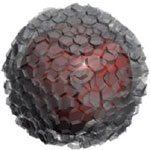 Graphene has attracted a huge amount of attention in recent years with its extraordinarily high electrical and thermal conductivities, mechanical, chemical properties, and large surface area. In order to meet the various demands for a variety of applications, preparation of desired structures of graphene sheets with controlled dimension and architecture are of significant importance. While research on flat graphene oxide structures has become quite common, there have been few reports on the preparation of hollow capsules of graphene through the nanosize, controlled assembly of graphene. Researchers in South Korea have now demonstrated the formation of graphene-based capsules through layer-by-layer (LbL) assembly of surface-functionalized reduced graphene oxide nanosheets of opposite charges onto polystyrene colloidal particles to produce multilayer thin films of graphene nanosheets.
Dec 14th, 2010
 A relatively new method of purifying brackish water is capacitive deionization (CDI) technology. The advantages of CDI are that it has no secondary pollution, is cost-effective and energy efficient. The basic concept of CDI, as well as electrosorption, is to force charged ions toward oppositely polarized electrodes through imposing a direct electric field: brackish water flows between pairs of high surface area carbon electrodes that are held at a potential difference of about 1-2 volts. The ions and other charged particles, such as microorganisms, are attracted to and held on the electrode of opposite charge. A research team has now developed a CDI application that uses graphene-like nanoflakes as electrodes for capacitive deionization. They found that the graphene electrodes resulted in a better CDI performance than the conventionally used activated carbon materials.
Oct 27th, 2010
 So far, there have been no research reports on a graphene-based transistor amplifier and investigations of its in-field controllability for analog, mixed-signal, and radio-frequency applications. Previous work on graphene transistors has largely focused on frequency multiplication near the Dirac point in graphene current-voltage characteristic. But now, a team of researchers has demonstrated the first triple-mode graphene amplifier. They have shown experimentally that by leveraging the ambipolarity of charge transport in graphene, the amplifier can be configured in the common-source, common-drain, or frequency multiplication mode of operation by changing the gate bias. This is the first demonstration of a single-transistor amplifier that can be tuned between different modes of operation using a single three-terminal transistor. Moreover, during its operation, the graphene amplifier was configured in-field to switch between the different modes. The result marks another important step toward graphene applications in electronics.
Oct 11th, 2010
 Current protein detection approaches are mainly dominated by heterogeneous immunological (or separation) assay methods. These assays are usually low-throughput and frequently require multiple steps including multiple incubation and careful washing of a surface onto which the labeled reagent has bound. In contrast, homogenous immunoassays can overcome these problems. In these assays, the signal is affected by binding and can often be run without a separation step. Such assays can frequently be carried out simply by mixing the reagents and sample and making a physical measurement. Researchers in China and Japan have now developed a graphene oxide based fluorescence assay for fast, ultra-sensitive, and selective detection of protein and demonstrated its use for detection of a prognostic indicator in early-stage cancer, cyclin A2.
Sep 13th, 2010
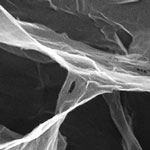 Given the massive interest and rapid developments in graphene research, scientists are now convinced that the controlled preparation of graphene-based materials with hierarchical and well-defined structures will pave the way for achieving high-performance applications of graphene in various technological fields such as optoelectronics, energy storage, polymer composites and catalysis. Self-assembly techniques have become some of the most effective strategies for this purpose. Although 2D self-assembly of graphene has been studied extensively from the perspectives of fundamental research and commercial applications, 3D self-assembly of 2D nanoscale graphene into functional macrostructures with well-defined networks remains as a great challenge and represents an important hurdle towards practical applications. Researchers in China have now provided a solution to this problem by demonstrating the successful preparation of self-assembled graphene hydrogel via a one-step hydrothermal process.
Jul 7th, 2010
 Subscribe to our Nanotechnology Spotlight feed