Showing Spotlights 281 - 288 of 336 in category All (newest first):
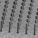 Graphene with its distinctive band structure and unique physiochemical properties - such as exceptionally low intrinsic electrical resistivity, high surface area, rapid electrode kinetics and good mechanical properties - is considered an attractive material for analytical electrochemistry. However, one of the key technical challenges for the use of graphene as functional material in device applications is the integration of nanoscale graphene onto micro- or millimeter sized sensing platforms. With a new methodology, a team from Florida International University was able to integrate graphene onto three-dimensional (3D) carbon microstructure arrays with good uniformity and controllable morphology.
Apr 24th, 2012
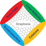 Graphene-based materials are emerging as highly attractive materials for real applications, especially in the area of energy conversion and storage. There are four major energy-related areas where graphene will have an impact: solar cells, supercapacitors, lithium-ion batteries, and catalysis for fuel cells. A recent review gives a brief overview of the recent research concerning chemical and thermal approaches toward the production of well-defined graphene-based nanomaterials and their applications in energy-related areas. But before graphene-based nanomaterials and devices find widespread commercial use, two important problems have to be solved: one is the preparation of graphene-based nanomaterials with well-defined structures, and the other is the controllable fabrication of these materials into functional devices.
Apr 18th, 2012
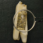 Early detection of pathogenic bacteria is critical to prevent disease outbreaks and preserve public health. This has led to urgent demands to develop highly efficient strategies for isolating and detecting this microorganism in connection to food safety, medical diagnostics, water quality, and counter-terrorism. A team of scientists has now developed a novel approach to interfacing passive, wireless graphene nanosensors onto biomaterials via silk bioresorption. The nanoscale nature of graphene allows for high adhesive conformality after biotransfer and highly sensitive detection. The team demonstrates their nanosensor by attaching it to a tooth for battery-free, remote monitoring of respiration and bacteria detection in saliva.
Mar 29th, 2012
 One of the greatest challenges in harnessing the power of nanotechnology is achieving dynamic control of mechanical, electronic, optical and chemical properties of nanoscale structures and devices. Dynamic control can be achieved through the use of piezoelectric materials. These are materials where applying a mechanical strain results in an electrical voltage or conversely, application of an electric field induces mechanical deformation. While piezoelectricity has mainly been shown for 3D bulk materials, the piezoelectric effect has also been demonstrated and exploited at the nanoscale. Researchers have now demonstrated through density functional theory calculations that piezoelectricity can be engineered into non-piezoelectric graphene by selective surface adsorption of atoms on only one side, which breaks inversion symmetry.
Mar 22nd, 2012
 Graphene is an excellent conductor of heat and might be an ideal material for thermal management in nanoelectronics. In field-effect transistors or interconnects most of the heat propagates directly below the graphene channel in the direction of the heat sink, that is, the bottom of a silicon wafer. For this reason, the highly thermally resistive silicon layers act as a thermal bottleneck, preventing the full utilization of graphene's excellent intrinsic properties. The breakdown current density in typical graphene devices is a hundred times larger than the fundamental limit in metals, which is set by electromigration. Researchers wanted to see if we can push the breakdown current density in graphene even further by better removal of dissipated heat. They managed to do it with the help of high-quality synthetic diamond. The graphene transistors or interconnects on synthetic diamond can sustain current densities which are a thousand times larger than in metals.
Feb 20th, 2012
 Noble metal nanoparticles such as gold, silver or platinum are widely used by scientists to develop novel applications in sensing, energy, spectroscopy, and catalysis. For instance, the combination of metal nanoparticles and carbon nanomaterials - graphene and nanotubes - has met with great interest in the area of biosensor applications as well as composite fabrication for light-energy conversion. In these applications, researchers make use of the formation of organic/inorganic hybrid nanosystems by incorporating metal nanoparticles in or onto the graphitic structures of carbon nanotubes or graphene. Researchers have now discovered a novel phenomenon whereby graphene can be catalytically transformed into carbon nanotubes by gold nanoparticles at relatively low temperatures.
Feb 8th, 2012
 Apart from graphene, other two-dimensional structures are also known to have unique properties which researchers are eager to exploit for novel nanotechnology applications in nanoelectronics and sensor or energy storage technology. Particular interest has been on semiconducting materials, such as molybdenum disulfide (MoS2), an abundant material in nature, which exhibits the unique physical, optical and electrical properties correlated with its single-layer atomic layer structure. Researchers have now fabricated a mechanically exfoliated single-layer MoS2 based phototransistor and investigated its electric characteristics in detail. These new findings show that, when compared with a 2D graphene-based device, the single-layer MoS2 phototransistor exhibits a better photoresponsivity.
Feb 3rd, 2012
 Thermal interface materials (TIMs) are essential ingredients of thermal management. TIMs are applied between the heat source, e.g. computer chips, and heat sinks and their function is to fill the voids and grooves created by imperfect surface finish of mating surfaces. Conventional TIMs filled with thermally conductive particles require high volume fractions of filler particles. But now, researchers have achieved a record enhancement of the thermal conductivity of TIMs by addition of an optimized mixture of graphene and multilayer graphene. The thermal conductivity of the epoxy matrix material was increased by an impressive factor of 23 at the 10 volume % of graphene loading. The epoxy-graphene composite preserved all the properties required for industrial TIM applications.
Jan 30th, 2012
 Subscribe to our Nanotechnology Spotlight feed