Showing Spotlights 521 - 528 of 628 in category All (newest first):
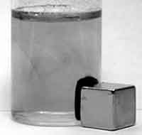 Probably any chemist must have dreamt about it: Quick isolation of a chemical from a reaction mixture without the hassle of tedious liquid handling lasting for hours. The problem is that today the product separation and postprocessing of organic compounds, proteins, nucleic acids, and natural products from complex reaction mixtures remains labor-intensive and costly. Catalytic processes in the liquid phase are important in many areas of the fine and specialty chemicals industries, and the use of solid catalysts means easier catalyst separation and recovery, hence facilitating their reuse. Usually a smaller catalyst particles means a higher activity, and sub micron particles are particularly attractive because they experience no significant attrition, i.e. no reduction in particle size. A major difficultly with small particles is the cumbersome fact that they are almost impossible to separate by conventional means, which can lead to the blocking of filters and valves by the catalyst. A possible solution to this problem is the magnetic separation of products from mixtures, as routinely applied in biochemistry. Unfortunately, the exorbitant price of magnetic microbeads and their low binding capacity limit their use for organic synthesis. Researchers in Switzerland, have now found a way to link organic molecules to metallic nanomagnets. This allows separating tagged molecules or reagents after synthesis within seconds. The technology is now explored in organic chemistry and biotechnology as an alternative to chromatography or crystallization. Combining classical organic synthesis or polymer production with magnetic separation could potentially revolutionize key processes in the chemical industry.
Sep 19th, 2007
 There is a huge demand for medical implants for almost every body part you can think of. As we have reported here before, the market for medical implant devices in the U.S. alone is estimated to be $23 billion per year and it is expected to grow by about 10% annually for the next few years. Implantable cardioverter defibrillators, cardiac resynchronization therapy devices, pacemakers, tissue and spinal orthopedic implants, hip replacements, phakic intraocular lenses and cosmetic implants will be among the top sellers. Current medical implants, such as orthopedic implants and heart valves, are made of titanium and stainless steel alloys, primarily because they are biocompatible. Unfortunately, in many cases these metal alloys with a life span of 10-15 years may wear out within the lifetime of the patient. With recent advances in industrial synthesis of diamond and diamond-like carbon film bringing prices down significantly, researchers are increasingly experimenting with diamond coatings for medical implants. On the upside, the wear resistance of diamond is dramatically superior to titanium and stainless steel. On the downside, because it attracts coagulating proteins, its blood clotting response is slightly worse than these materials and the possibility has been raised that nanostructured surface features of diamond might abrade tissue. That's not something you necessarily want to have in your artificial knee or hip joints (although some of the currently used implant materials cause problems as well). Researchers have now run simulations that show that thin layers of ice could persist on specially treated diamond coatings at temperatures well above body temperature. The soft and hydrophilic ice multilayers might enable diamond-coated medical devices that reduce abrasion and are highly resistant to protein absorption.
Sep 18th, 2007
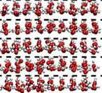
 Zinc Oxide (ZnO) has long been used in its powdered form as pigments in paints, coatings for papers, in the commercial manufacture of rubber goods as well as UVA and UVB blocker and mild antimicrobial in cosmetics. ZnO is also one of the most important semiconductor compounds and numerous reports have been documented in the literature about the preparation and characterization of ZnO nanocrystals. While polycrystalline forms of ZnO have been used for technical uses such as piezoelectric transducers, light emitting diodes, and transparent conducting films, the progress in developing single crystal bulk ZnO have brought its promise as a wide band gap semiconductor to the fore. Superstructures formed from ZnO nanocrystal quantum dots may find applications in various areas such as optics, electronics and magnetism. For these 2D and 3D superstructures to be useful they need to be well-ordered. Usually, nanocrystals without any surface modification are less stable and they usually undergo aggregation or crystal growth, and consequently it is rather hard for bare nanocrystals to self-assemble into 2D, and especially into 3D, ordered structures. So far, most well-ordered assemblies of nanocrystals have been prepared through a surface modification approach. Efforts have been made to prepare superstructures composed of ZnO nanocrystals but it is rather challenging to obtain well-ordered 3D ZnO superlattices. Researchers in China have now found that ZnO nanocrystals capped with ionic liquids spontaneously assemble into a three-dimensional lattice. Apparently, simply drying a solution of the modified ZnO nanocrystals is all that is needed for the superlattice to form. The presence of the ionic liquid prevents the nanocrystals from aggregating.
Sep 12th, 2007
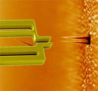 Hands-on nanotechnology: towards a nanorobotic assembly line (Nanowerk Spotlight) Until the twentieth century, a single craftsman or team of craftsmen would normally create each part of an industrial product individually and assemble them together into a single item, making changes in the parts so that they would fit together and work together; the so-called English System of manufacture. Then Henry Ford came along and in 1907-08 developed the assembly line for his Model T automobile. This innovation revolutionized not only industry but also our society because it allowed mass production of industrial goods at much lower cost than before. At its core, an assembly line is a manufacturing process in which interchangeable parts are added to a product in a sequential manner to create a finished product. Nanotechnology techniques today are pretty much where the industrial world was before Ford's assembly line - a domain of craftsmen and not of mass production. It has long been a dream for nanotechnologists that robots could one day be used in a similar way to produce nanodevices. A group of researchers from Denmark and Germany have now developed the rudimentary beginnings of the nanotechnology equivalent of an assembly line. They have shown 'pick-and-place' assembly of a working device using a silicon gripper - a robotic 'hand' some 10000 times smaller than a human hand. This nanogripper, controlled by a nanorobotic arm, is capable of picking up a carbon nanofiber (CN) and fix it onto the tip of an atomic force microscope cantilever.
Sep 11th, 2007
 For the builders and engineers among you, our subject today is cement. Not necessarily a material one would associate with high-tech, not to mention nanotechnology. However, it's probably fair to say that our modern society is built on cement. Look around you and you'll find it everywhere - in buildings, roads, bridges, dams. Early construction cement (the word goes back to the Romans who used the term opus caementitium to describe masonry which resembled concrete and was made from crushed rock with burnt lime as binder) probably is as old as construction itself. So what is it? Cement, as it is commonly known, is a mixture of compounds made by burning limestone and clay together at very high temperatures. Cement is then used, together with water, as binder in a synthetic composite material known as concrete. For concrete to obtain its optimal properties it needs to harden. And that takes time. For builders, time is money and particularly in industrial settings time is a major cost issue. Time is also a safety and convenience factor, think about infrastructure repair work on roads and dams for instance. Cement manufacturers have already known that reducing the particle size of cements results in faster-binding formulations. By taking the ultimate reduction down to the nanoscale, researchers in Switzerland have shown that a one-step preparation of nanoparticulate cement with a conventional Portland cement composition results in a drastically increased early reactivity of the cement.
Sep 10th, 2007
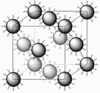
 In order to exploit the unique properties of nanoscale materials for advanced applications it is often necessary to assemble nanoparticles into arrays with specific architectures. The interaction among the nanoparticles, or effects arising from their assembled larger structure, could result in interesting optical, magnetic or catalytic properties that researchers and engineers then could exploit for new materials and applications. In recent years, there has been much interest in colloidal crystals - which are examples of periodic nanoparticle arrays - as photonic crystals, templates for photonic crystals, sensors, optical and electrooptical devices, and as model systems to study crystallization processes. The success of many of these potential applications is currently limited by scientists' ability to control the structure of colloidal crystals. Normally, crystallization of uniform colloids produces face-centered cubic or hexagonal close-packing. A few other colloidal crystal structures have recently been reported, but they either require careful balance of electrostatic interactions between colloidal particles, or they rely on directing nanoparticles on a lithographic pattern that then dictates the geometry of a few layers in a thin film. New research now has resulted in a completely different and novel approach of colloidal crystallization that results in simple cubic colloidal crystals extending over many unit cells in three dimensions. Simple cubic packing is quite rare, even in atomic structures. Here, it results from combined disassembly and self-reassembly of a template- directed structure in a single reaction step.
Sep 6th, 2007
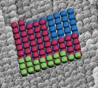
 When Gutenberg built his printing machine with moveable type in the mid 15th century, little idea did he have that he started the information age; even less that scientists would adopt the process to the nanoscale. The printing press went through several revolutionary improvements such as Lanston's monotype machine (1884), Mergenthaler's linotype machine (1886), the photo-typesetting process developed in the 1960s and finally digital printing in the 1980s. Today, printing is the most widespread technology to deposit small particles onto various surfaces. Commercial desktop laser printers use toner particles with a few microns in size while top of the line high-priced industrial printing machines sometimes already use sub-micron size particles. On the other hand, the precise positioning of nanoparticles on surfaces is key to most nanotechnology applications especially nanoelectronics. However, for automated patterning of particles, existing methods are either slow (e.g., dip-pen lithography) or require prefabricated patterns on the target substrate (e.g. for electrostatic positioning). Using a process akin to the printing press, researchers already have managed to bypass the need for epitaxial growth or wafer bonding to integrate wide ranging classes of dissimilar semiconducting nanomaterials onto substrates for the purpose of constructing heterogeneous, three dimensional electronics. Scientist in Switzerland have now developed a parallel method for the assembly and integration of a large number of bulk-synthesized nanoparticles onto an unstructured surface with high resolution and yield.
Sep 5th, 2007
 You might have come across the acronym NBIC, which stands for Nanotechnology, Biotechnology, Information technology and new technologies based on Cognitive science. Initially introduced in the U.S. National Science Foundation's 'Converging Technologies for Improving Human Performance' report this acronym is often used to describe the basic idea that scientific and technological innovation can be stimulated through the convergence of two, three, or all four fields. At its most radical (and most controversial), proponents of convergence suggest that nanotechnologies will promote the unification of most branches of science and technology, based on the unity of nature at the nanoscale, including cognitive sciences. We'll keep you posted on this over the next few decades and see how it all works out. For the time being, though, it would be nice to be able to report on something more hands-on and - dare I write it - even practical. As it happens, scientists at the University of Toronto have done exactly that. They have demonstrated, for what appears to be the first time, the convergence of nanotechnology, microtechnology, microfluidics, photonics, signal processing, and proteomics to build a medical device that could lead to the development of fast, portable point-of-care diagnostics for infectious disease (IDs) such as HIV, SARS and many others.
Aug 31st, 2007
 Subscribe to our Nanotechnology Spotlight feed