Showing Spotlights 25 - 32 of 161 in category All (newest first):
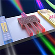
 Blackbody response is highly desired in two-dimensional (2D) infrared photodetectors, which determines their practical applications. However, limited by the thickness and complex defects of 2D materials, 2D photodetectors still suffer from problems such as low quantum efficiency and large dark current. Researchers now demonstrate fully depleted self-aligned van der Waals (vdW) photodetectors based on a heterosandwiched structure.
Sep 2nd, 2022
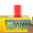
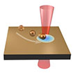
 One convenient way to manipulate nanoscale objects with remote controllability is actuation and propulsion by light, which is largely based on optical and photothermal-induced forces. Unfortunately, the output of optical and photothermal-induced forces is small and speed is slow. This changes with a novel and intriguing nanoactuation system: plasmonic nanodynamite. This system can be optically triggered to eject gold nanobullets with an initial speed of up to 300 m/s.
Aug 8th, 2022
 Spontaneous charging of interfaces between water and hydrophobic media is a mysterious feature whose nature and origin - despite many efforts to explain them - are still not fully understood. Many spectroscopic results and interpretations along with computational work are not consistent with one another and a consensus on the nature and origin of interfacial charging has not been reached. A clear understanding of this puzzling phenomenon needs a variety of approaches from diverse perspectives, which, hopefully will all add up and be pieced together towards a complete description of the full picture.
Jul 7th, 2022
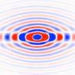
 Ultra-narrow optical features with a spectral bandwidth below 1 megahertz are highly sought-after for applications in ultrahigh-precision sensing, narrow-band filtering, and information storage for optical computing - but unfortunately they are extremely challenging to generate. But now there is a novel way to achieve ultra-narrow optical features. And unlike conventional approaches, it is cost-effective, has a simple arrangement, and is loss-free, while offering on-demand tunability and ultrahigh sensitivity.
Jun 17th, 2022
 Polaritons in biaxial crystals offer a promising route to manipulate nanoscale light-matter interactions. The dynamic modulation of their dispersion is of great significance for future integrated nano-optics but remains challenging. Researchers theoretically demonstrate and experimentally verify such tailored polaritons at the interface of heterostructures. The interface engineering may shed new light on programmable polaritonics, energy transfer, and neuromorphic photonics
Apr 22nd, 2022
 The concepts of metamaterials and metasurfaces have spawned massive novel applications in free-space optics. However, recent research also indicates that they possess prominent potential for tailoring the electromagnetic modes in optical waveguides. In a new review, researchers discuss recent advances of applying various meta-structures with diverse waveguide platforms to enhance the performance and expand functionalities for integrated photonic devices.
Dec 2nd, 2021
 Optical tweezers used to trap nanoscale objects usually require a tightly focused laser beam with high optical intensity. The problem with all conventional laser-based optical manipulation techniques is that the laser light could cause photodamages and photothermal degradation to nanoparticles and biological samples. A novel solution to this problem creates a low-temperature spot in the solution and trap particles and molecules at the cold spot. This new technique can effectively avoid photothermal damages.
Jun 29th, 2021
 Relying on the quantum confinement effect, the strong light-matter interaction in low-dimensional materials enables them to exhibit excellent photodetection. The unique out-of-plane van der Waals force in low-dimensional layered materials makes them free from the surface dangling bonds compared to traditional bulk materials, which reduces the dark current of the devices by eliminating surface recombination. These unique advantages make low-dimensional materials have the potential to achieve breakthroughs in the field of low-cost high-performance room-temperature infrared detection.
Jun 7th, 2021
 Subscribe to our Nanotechnology Spotlight feed