Showing Spotlights 2577 - 2584 of 2851 in category All (newest first):
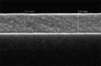 A few years ago it was discovered that the process of thermal inkjet printing can be applied to fabricate hard tissue scaffolds (such as bones) and, just recently, soft tissue with liquid biomaterials. Research is also underway to use inkjet printing for the fabrication of organic semiconductors, which, because of their low stability, will be targeted at one-time-only applications such as water purity testers. Compared to the research done with respect to organic materials, inkjet printing of inorganic materials for the formation of active devices is relatively rare. To date, only a handful of inorganic materials have been inkjet printed, primarily because of the difficulty in preparing inkjet-printable precursors. Current methods for the production of functional inorganic electronic devices are quite expensive because they require the sequential deposition, patterning, and etching of selected semiconducting, conducting, and insulating materials, involving multiple photolithography and vacuum-deposition processes. Now though, researchers have come up with a process for printable inorganic semiconductors, opening a route to the fabrication of high-performance and ultra low-cost electronics such as transparent electronics and thin film solar cells.
Mar 20th, 2007
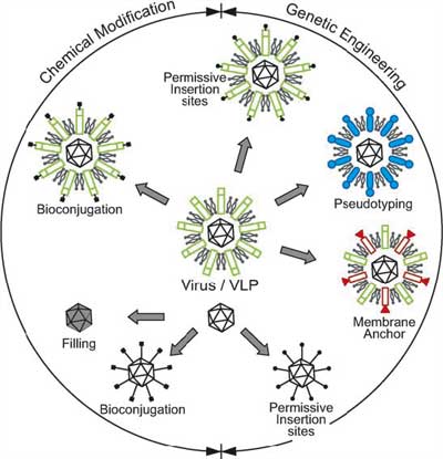 Geneticists regularly use viruses as vectors to introduce genes into cells that they are studying. Viruses are also the most common carrier vehicles in gene therapy. Having been genetically altered to carry normal human DNA, they deliver the therapeutic genes to the patient's target cells. These viruses infect cells, deposit their DNA payloads, and take over the cells' machinery to produce the desirable proteins. Current trends in nanotechnology promise to take virus technology into an entirely new direction. From the viewpoint of a materials scientist, viruses can be regarded as organic nanoparticles. Their surface carries specific tools designed to cross the barriers of their host cells. The size and shape of viruses, and the number and nature of the functional groups on their surface, is precisely defined. As such, viruses are commonly used in materials science as scaffolds for covalently linked surface modifications. The powerful techniques developed by life sciences are becoming the basis of engineering approaches towards nanomaterials, opening a wide range of applications far beyond biology and medicine.
Mar 19th, 2007
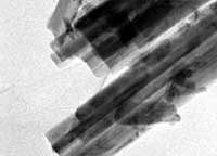
 The assembly of nanoparticles along the external or internal surface of carbon nanotubes (CNTs) is of both fundamental and technological interest. Combining unique properties of CNTs and nanoparticles, the nanoparticle/nanotube composite structure attracts a broad range of advanced applications, including nanoelectronics, chemical and biosensors, catalysis and fuel cells. This so-called 'decoration' of CNTs has been used to increase the hydrogen storage capacity, to make nanotubes magnetic, or to grow secondary structures inside the nanotubes to increase the available surface for catalysis. In the case of interior wall decoration of CNTs, the internal cavity of the nanotube often is obstructed and no flow can be achieved or there could be release of the particles in the environment. In the case of exterior wall decorations, the particles enter in direct contact with the environment and may be lost during the nanotube handling. A novel technique of multifunctional nanotubes with controllable amounts of nanoparticles embedded in their walls during the synthesis process solves both problems leaving the CNT bore accessible and keeping the nanoparticles shielded from the environment by the CNT walls. This paves the way to using carbon nanotubes as nanoscale biological probes for sub-cellular investigation.
Mar 16th, 2007
 Carbon nanotubes (CNTs) have captured the imagination of many scientists and engineers as a result of properties of individual tubes (e.g. very high electrical and thermal conductivities, high stiffness). Things often get 'messy' however, when one tries to make them work collectively, e.g. in composites. Three-dimensional networks of carbon nanotubes are usually made within a supporting material, such as in polymer composite or liquid dispersion. While networks of CNTs have been observed transiently in furnaces with lots of raw nanotube material, such an approach does not permit much experimental control over the resulting network. A novel approach to fabricating CNT networks are CNT aerogels. Aerogels are novel materials in their own right - a material derived from gel in which the liquid component of the gel has been replaced with gas. The result is an extremely low density solid. Microscopically, aerogels are composed of tenuous networks of clustered nanoparticles. These materials often have unique properties due to their very high strength-to-weight and surface-area-to-volume ratios. To date, most aerogels are fabricated from silica or pyrolized organic polymers. Fabricating aerogels with CNTs offers potential for improvement over current carbon aerogel technologies in device applications such as sensors, actuators, electrodes, and thermoelectrics.
Mar 15th, 2007
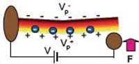 Piezoelectricity is a coupling between a material's mechanical and electrical behavior. When a piezoelectric material is squeezed, twisted, or bent, electric charges collect on its surfaces. Conversely, when a piezoelectric material is subjected to a voltage drop, it mechanically deforms. Many crystalline materials exhibit piezoelectric behavior and when such a crystal is mechanically deformed, the positive- and negative-charge centers are displaced with respect to each other. So while the overall crystal remains electrically neutral, the difference in charge center displacements results in an electric polarization within the crystal. Electric polarization resulting from mechanical deformation is perceived as piezoelectricity. This phenomenon was discovered by the brothers Pierre and Jacques Curie in 1880 and the word is derived from the Greek piezein, which means to squeeze or press. The piezoelectric effect finds useful applications such as the production and detection of sound, generation of high voltages, electronic frequency generation, microbalance, and ultra fine focusing of optical assemblies. For instance, types of piezoelectric motor include the well-known traveling-wave motor used for auto-focus in reflex cameras. A new research field, nanopiezotronics refers to generation of electrical energy at the nanometer scale via mechanical stress to the nanopiezotronic device. For example, bending of a zinc oxide nanowire transforms that mechanical energy into electrical energy. This new approach has the potential of converting biological mechanical energy, acoustic/ultrasonic vibration energy, and biofluid hydraulic energy into electricity, demonstrating a new pathway for self-powering of wireless nanodevices and nanosystems.
Mar 14th, 2007
 The challenges in transportation security, most notably air transport, evolve around detecting explosives before they reach their target, i.e. get on a plane for instance. The two technology-based methods of explosive detection are either nuclear-based (probing the screened object with highly penetrating radiation) or rely on trace detection. Trace detection techniques use separation and detection technologies, such as mass spectrometry, gas chromatography, chemical luminescence, or ion mobility spectrometry, to measure the chemical properties of vapor or particulate matter collected from passengers or luggage. All these methods require bulky and expensive equipment, costing hundreds of thousands of dollars apiece. This results in a situation where the effort and technology involved in the detection of explosives are orders of magnitude more expensive than the effort and costs incurred by terrorists in their deployment. Today, the cheapest, very reliable, and most mobile form of explosive detection is decidedly low-tech - dogs. The olfactory ability of dogs is sensitive enough to detect trace amounts of many compounds, which makes them very effective in screening objects. A dog can search an entire airport in a couple of hours. Using a chemical analysis machine would mean wiping down nearly every surface in the airport with a sterile cotton pad, then sticking those pads, one by one, into a computer for analysis. Given the recent advances of nanotechnology, researchers are now trying to develop the next generation of explosives sensors that are accurate, fast, portable and inexpensive - and don't need to be fed.
Mar 13th, 2007
 It seems that with every new study on the toxicity of nanomaterials there remain more questions afterwards than before. Environmental, occupational and public exposure to engineered nanoparticles will increase dramatically in the near future as a result of the widespread use of nanoparticles for consumer and industrial products. The extent of future exposure to nanoparticles associated with these new products is still unknown. So far only limited data is available regarding carbon nanotube (CNT) toxicity. As a result still not much is known about their impact on biological systems including humans. Discussions regarding the potential risks of their widespread use, as well as their possible positive impact are just beginning to take place. In order to provide a basis for comparison to existing epidemiological data, a group of researchers in Switzerland and Germany have investigated CNTs at various degrees of agglomeration using an in vitro cytotoxicity study with human cancer cells. The cytotoxic effects of well-dispersed CNT were compared with that of conventionally purified rope-like agglomerated CNTs and asbestos as a reference. While suspended CNT-bundles were less cytotoxic than asbestos, rope-like agglomerates induced more pronounced cytotoxic effects than asbestos fibers at the same concentrations. The study underlines the need for thorough materials characterization prior to toxicological studies and corroborates the role of agglomeration in the cytotoxic effect of nanomaterials.
Mar 12th, 2007
 Since their discovery in the early 1990s, carbon nanotubes (CNTs) and carbon nanofibers (CNFs) have been used in a wide variety of applications. They have become indispensable in nanosciences and nanotechnology. However, because their production on an industrial scale remains expensive, their commercial use in such areas as catalysis has remained unthinkable. Current production processes including preparation of the support, normally silica or alumina, and impregnation with catalytically active metal for hydrocarbon decomposition, are not suitable for mass production. Researchers in Germany now report the fabrication of carbon nanotubes and carbon nanofibers on Mount Etna lavas used both as support and as catalyst, the first step for industrial production without preparation of support and its wet-chemical treatment. Such fabrication of CNTs/CNFs on naturally occurring minerals without synthetically prepared catalyst could pave the way for further exploitation of the superior properties of tailored nanostructured carbon for large-scale applications, such as catalysis and water purification by adsorption.
Mar 9th, 2007
 Subscribe to our Nanotechnology Spotlight feed