Showing Spotlights 2473 - 2480 of 2838 in category All (newest first):
 Children begin to learn by seeing, hearing, tasting and, above all, by touching. In a very similar approach, we are currently learning to orient ourselves in the nanoworld by 'feeling' materials - not with our fingers, but with microscopes that allow us to probe these materials with atomic resolution.
Aug 7th, 2007
 One of the many fascinating concepts in nanotechnology is the vision of molecular electronics. If realized, the shift in size from even the smallest computer chip today would be staggering - a quantum leap, so to speak (literally). Look at it this way: a single drop of water contains more molecules than the billions and billions of silicon chips ever produced. Molecular electronics engineers of tomorrow might use individual molecules to perform the functions in an electronic circuit that are performed by semiconductor devices today. Don't get your hopes up, though, that your next iPod will be truly nano. Scientists today are still struggling with the most basic requirements for molecular electronics, for instance, how to precisely and reliably position individual molecules on a surface. DNA-based nanostructuring is one approach that could lead to promising results. It has already been shown that DNA could be used to structure nanoscale surfaces. Now, a team in Germany has demonstrated that nanoscale objects of very different size can be deposited simultaneously and site-selectively onto DNA-displaying surfaces, based on sequence-specific DNA-DNA duplex formation.
Aug 6th, 2007
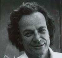 Having just re-read Richard Feynman's 20-year old autobiography titled Surely You're Joking, Mr. Feynman! (Adventures of a Curious Character) I thought it makes for a great little Nanowerk Spotlight leading into the weekend - and it won't be about nanotechnology. Feynman's 1959 lecture "Plenty of room at the bottom" is probably the most famous and most quoted physics speech ever and it is the one thing that most non-scientists associate with his name. Feynman, who received the Nobel Prize in Physics in 1965 for his work on on quantum electrodynamics, participated in the Manhattan Project and was a member of the panel that investigated the Space Shuttle Challenger disaster in 1986. He taught physics, first at Cornell and later at the California Institute of Technology. In typical Feynman fashion, a major factor in his decision of chosing CalTech over other institutions was a desire to live in a mild climate, a goal he chose while having to put snow chains on his car's wheels in the middle of a snowstorm in Ithaca, New York. What makes this book such a gem is the weird and wacky collection of anecdotes that Feynman serves up when leading us through his childhood, education and career. Whether he learns how to pick locks and crack safes, plays the bongo drums in an orchestra, gets a commission to paint a naked female toreadore, or competes in a samba competition during Carnival in Rio, the book is not about physics, but the physicist. Underneath all these hilarious stories, though, are recurring leitmotifs of curiosity, tenacity, and total disrespect for ideas that have no grounding in science. For everyone who is quoting Feynman's speech, or who is reading it, this autobiography goes a long way explaining the unconventional mind behind his revolutionary ideas.
Aug 3rd, 2007
 The question if certain engineered nanoparticles are toxic, and if yes to what degree, is still one of the major issues that hasn't been properly answered yet. Most studies in the literature thus far have focused on the environmental aspects of nanoparticle toxicity, and these studies have been conducted primarily on industrial or natural/incidental nanoparticles. However, engineered nanoparticles are at the forefront of the rapidly developing field of nanomedicine; and here they are deliberately injected into the body to perform a specific medical application: fluorescent agents for imaging; drug delivery vehicles; or therapeutic agents for the destruction of cancer cells (for instance in thermolysis); just to name a few. A brand new review article provides the first comprehensive summary of the properties of engineered nanoparticles which determine their interaction with components of the immune system. It concludes that nanoparticle-based therapeutics are no more intrinsically immunotoxic than traditional pharmaceuticals, such as biotechnology-derived or small molecules. Moreover, incorporation of traditional drugs into nanotechnology formulations frequently results in a decrease in immunotoxicity compared to the native drug. Although many questions still require thorough investigation, the available data suggest that nanoparticles can be engineered to become the next generation of biocompatible drug delivery platforms.
Aug 2nd, 2007
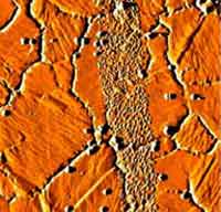
 You might remember our Spotlight from a few months ago (25 years of scanning probe microscopy and no standards yet) where we gave an overview of how scanning probe microscopy has flourished over the past 25 years. The most versatile implementation of the scanned probe principle is the atomic force microscope (AFM). It has become one of the foremost tools for imaging, measuring and manipulating matter at the nanoscale. The essential part of an AFM is a microscale cantilever with a sharp tip (probe) at its end that is used to scan the specimen surface. The cantilever is typically silicon or silicon nitride with a tip radius of curvature on the order of nanometers. When the tip is brought into proximity of a sample surface, forces between the tip and the sample lead to a deflection of the cantilever according to Hooke's law. A multi-segment photodiode measures the deflection via a laser beam, which is reflected on the cantilever surface. Because there are so many promising areas in nanotechnology and biophysics which can be examined by AFM (force spectroscopy on DNA, muscle protein titin, polymers or more complex structures like bacteria flagella, 3-D imaging, etc. ) the availability of instruments is crucial, especially for new groups and young scientists with limited funds. The price tag of AFMs runs in the hundreds of thousand s of dollars, though. Until now, AFM heads are made of metal materials by conventional milling, which restricts the design and increases the costs. German researchers have shown that rapid prototyping can be a quicker and less costly alternative to conventional manufacturing.
Aug 1st, 2007
 Ever since Roman glass blowers made the Lycurgus cup, some 2,400 years ago, researchers and engineers have figured out to do all kinds of things with light, be it in optical fiber communications; the use of lasers for welding, cutting and surface modification of materials; photonic gyroscopes in aviation; or optical switches in computing. As a general field of science, photonics defines the knowledge devoted to the generation, transmission, detection, control and handling of light. One sub-domain, nanophotonics deals with the manipulation and emission of light using nanoscale material and devices. One of the sizzling hot topics within nanophotonics is plasmonics, which holds the promise of a class of subwavelength-scale optoelectronic components that could form the building blocks of a chip-based optical device technology that is scaleable to molecular dimensions. Here, we report on the latest achievements of a Spanish-French group of researchers that brings the exiting concept of an optically driven lab-on-a-chip closer.
Jul 31st, 2007
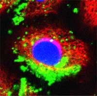 Recent developments in spectroscopic techniques allow highly sensitive image detection both in vitro and in vivo on the individual cell level. These methods depend on nanometer-size particles as detection probes. One class of such particles, so-called nanocrystals or quantum dots (qdots), is very popular for constructing detection probes for biolabeling. Scientists have discovered that these nanocrystals can enable researchers to study cell processes at the level of a single molecule and may significantly improve the diagnosis and treatment of diseases such as cancers. Qdots are either used as active sensor elements in high-resolution cellular imaging, where the fluorescence properties of the qdots are changed upon reaction with the analyte, or in passive label probes where selective receptor molecules such as antibodies have been conjugated to the surface of the dots. Qdots could revolutionize medicine. Unfortunately, most of them are toxic. Ironically, the existence of heavy metals in qdots such as cadmium, a well-established human toxicant and carcinogen, poses potential dangers especially for future medical application, where qdots are deliberately injected into the body. As the use of nanomaterials for biomedical applications is increasing, environmental pollution and toxicity have to be addressed, and the development of a non-toxic and biocompatible nanomaterial is becoming an important issue. Researchers are now proposing the use of nanoscale diamond particles as a non-toxic alternative to heavy metal qdots.
Jul 30th, 2007
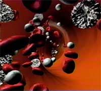
 Inhalation, or respiratory, therapy is a fairly old discipline of medicine that dates back to ancient times (and not always for purely therapeutic effects; witness the hookah). In the late 18th century, earthenware inhalers became popular for the inhalation of air drawn through infusions of plants and other ingredients and about 50 years ago the first pressurized metered dose inhaler was put on the market. Especially people suffering from asthma are very familiar with inhalers - devices that help deliver a specific amount of medication to the lungs. The delivery of drugs via the pulmonary route is a potentially effective form of therapy not only for asthma but also for for patients with other chronic diseases, including the debilitating hereditary disease, cystic fibrosis, type I diabetes (insulin is absorbed well through the lungs), and recently lung cancer. During inhalation therapy the drugs are delivered in aerosol form, meaning that very small particles of the drug are suspended in air (liquid particles make mist, solid particles make fume or dust). Unfortunately, state the-of-the-art aerosol delivery technologies do not allow to target aerosols to specific regions of the lung. Researchers in Germany now have show that aerosols containing magnetic nanoparticles can be guided inside the lungs and thus offer a potential new route for lung cancer treatment.
Jul 27th, 2007
 Subscribe to our Nanotechnology Spotlight feed