Showing Spotlights 17 - 24 of 110 in category All (newest first):
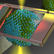
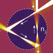 Modern-day electronics or communication technology would not exist without electron microscopy, and the same can be said for many other types of technology. Beyond imaging, the focused beam of electrons is also used for analysis of the chemical composition, the crystal structure, and many other useful things. In new work, researchers have proposed to use graphene as a two-dimensional vacuum chamber, and build a two-dimensional electron microscope, where the electrons fly from the electron gun to the target without ever leaving the graphene sheet.
Jun 9th, 2017
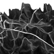
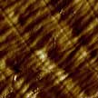 Caenorhabditis elegans, a free-living soil nematode, has become an important experimental model for biomedical research. This nematode has been successfully employed in genetics, ageing research, behavioral assays, drug screening and (nano)toxicology. In a new study, researchers report for the first time the effective imaging of the nanoscale structure of C. elegans nematodes' cuticle using atomic force microscopy operating in PeakForce Tapping mode. This mode allows imaging C. elegans nematodes both in air and in their native liquid environment.
Nov 16th, 2016
 Over the past few decades, the development of electron microscopy has gone hand in hand with techniques for atomically precise fabrication of 3D structures based on electron and ion beams. A recent review article illustrates the use of focused electron and ion beams (e-beams and i-beams) to induce highly localized chemical reactions at solid-vapor and solid-liquid interfaces, amorphous to crystalline phase transformations with atomic layer precision, and the motion of specific single dopant atoms within crystal lattices, thus laying the foundation for atomically precise directed assembly of materials and devices.
May 31st, 2016
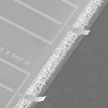
 The drawbacks of existing measures for calibrating scanning probe microscopes (SPMs) based on various diffraction gratings and periodic microstructures, are large period and large error of period. Both factors prevent using these measures for precise calibration of SPMs and other instruments operating in the nanometer range. To address this issue, researchers have developed a method of calibration of a scanning probe microscope by lattice constant of a crystal.
Mar 25th, 2016
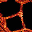
 Catalytic nanoparticles play a crucial role in accelerating chemical reactions by offering their active sites and surfaces. Fine-tuning their surface structure during synthesis and phase transformations can enhance their catalytic activity and durability by manifolds. However, control and feedback on the synthesis/transformation studies demand characterization techniques that can provide structural and compositional information on the atomic level.
Nov 24th, 2015
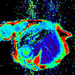 Imagine the possibility of non-invasive, non-radiation based Magnetic Resonance Imaging (MRI) in combating cardiac disease. Researchers are developing a process that would use nanotechnology in a novel, targeted approach that would allow MRIs to be more descriptive and brighter, and to target specific organs. By using nanoparticle-based MRI positive contrast agents, you can specifically target different tissues or organs, you can control active component loading, and you can generate bright or hyperintense anatomical view of the tissue.
Nov 11th, 2015
 The development of nanoscale devices and applications requires ultra-sensitive sensing systems that can offer not only atomic resolution imaging but also sub nanometer scale displacement detection, zeptogram level mass sensing, or single bio-molecular sensing. Researchers have now developed a novel sensor that addresses some of the shortcomings that have plagued existing optical scanning systems , namely size, complexity, and cost. This sensing technology is completely electrical and capable of sensing very small displacement as low as in the femtometer range.
Sep 30th, 2015
 Researchers report a non-destructive and high throughput 3D imaging of carbon nanotubes (CNTs) embedded in polymer matrix via Scanning Electron Microscopy (SEM). While have been several open questions remaining for SEM subsurface imaging of CNTs, this new findings clarify these issues and help establish SEM subsurface imaging as a useful and facile method to provide quantitative 3D information on CNT dispersions in polymer composites.
Feb 18th, 2015
 Subscribe to our Nanotechnology Spotlight feed