Showing Spotlights 2369 - 2376 of 2838 in category All (newest first):
 Ever since the nanoworld got excited over carbon nanotubes there has been great interest, and progress, in the development of new nanotubes based on metal oxides, sulfides, nitrides, elemental species and others. The characteristic that all these tubular structures have in common is a hollow morphology which may possess circular, or square-like or hexagonal-like cross section. In a standard tubular structure, a cavity is located at the center and extends over the entire length, so that the tube cavity and the tube wall have the same symmetry axis. Structures in which an internal cavity strongly deviates from the center of symmetry towards one side are rather rare. Researchers have now synthesized novel, unconventional nanotubes that are distinctly different from any previously reported nano- and microtubes. These tubes display flattened and thin belt- or ribbon-like morphologies, which are not common for any known tubular structures. This may represent a new, interesting growth phenomenon for tubular crystal structures.
Jan 11th, 2008
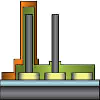 A memory chip is an integrated circuit made of millions of transistors and capacitors. In the most common form of computer memory, dynamic random access memory (DRAM), a transistor and a capacitor are paired to create one memory cell, which represents a single bit of data. The capacitor holds the bit of information, either a 0 or a 1. The transistor acts as a switch that lets the control circuitry on the memory chip read the capacitor or change its state. Because each bit stored in a chip is controlled by one transistor, memory capacities tend to expand at the same pace as the number of transistors per chip - which still follows Moore's Law and therefore currently doubles every 18 months. The problem is that the capacitor - consisting of two charged layers separated by an insulator - can shrink only so far. The thinner insulators get the more they allow charges to tunnel through. Tunneling increases the leakage current, and therefore the standby power consumption. Eventually the insulator will break down. Researchers have been trying to develop electromechanically driven switches that can be made small enough to be an alternative to transistor-switched silicon-based memory. Electromechanical devices are suitable for memory applications because of their excellent ON-OFF ratios and fast switching characteristics. With a mechanical switch there is physical separation of the switch from the capacitor. This makes the data leakage problem much less severe. Unfortunately they involve larger cells and more complex fabrication processes than silicon-based arrangements and therefore have not been so far an alternative to scaling down beyond semiconductor transistors. Researchers now have reported a novel nanoelectromechanical (NEM) switched capacitor structure based on vertically aligned multiwalled carbon nanotubes (CNTs) in which the mechanical movement of a nanotube relative to a carbon nanotube based capacitor defines ON and OFF states.
Jan 10th, 2008
 The UK government has published its second research report on nanotechnology risks, outlining progress on its research agenda to address the potential risk posed by the products of nanotechnology. The report places the UK research program in an international context. The Nanotechnology Research Coordination Group (NRCG) is collaborating with international partners, particularly through the Organization for Economic Co-operation and Development (OECD) and the International Standards Organization (ISO), to share data and experiences. In this way they hope to be able to maximize the effectiveness and speed with which potential risks may be identified and managed. The report also responds to the recommendations made by the Council for Science and Technology (CST) review (March 2007) on the UK research program and the activities of the NRCG.
Jan 9th, 2008
 For centuries, man has searched for miracle cures to end suffering caused by disease and injury. Many researchers believe nanotechnology applications in medicine may be mankind's first 'giant step' toward this goal. According to Freitas nanomedicine is "...(1) the comprehensive monitoring, control, construction, repair, defense, and improvement of all human biological systems, working from the molecular level, using engineered nanodevices and nanostructures; (2) the science and technology of diagnosing, treating, and preventing disease and traumatic injury, of relieving pain, and of preserving and improving human health, using molecular tools and molecular knowledge of the human body; (3) the employment of molecular machine systems to address medical problems, using molecular knowledge to maintain and improve human health at the molecular scale." Nanomedicine not only has the potential to change medical science dramatically but to open a new field of human enhancements that is poised to add a profound and complex set of ethical questions for health care professionals. For instance, there is a fine line between medical and non-medical uses of nanotechnology for diagnostic, therapeutic and preventive purposes (e.g. non-medical implants in soldiers). The question of whether nanotechnology should be used to make intentional changes in or to the body when the change is not medically necessary is just one hot topic in a long list of concerns. The good news is that these questions are being asked, but there is still much work to be done, but despite the enormous promise of nanomedicine, and the considerable funding going into the field, the research into the ethical, legal and social implications of nanomedicine is comparatively minute. As Peter Singer wrote in his 2003 tutorial Mind the gap: science and ethics in Nanotechnology: 'The science leaps ahead, the ethics lags behind.' As with nanotechnology in general, there is danger of derailing nanomedicine if the study of ethical, legal and social implications does not catch up with scientific developments.
Jan 8th, 2008
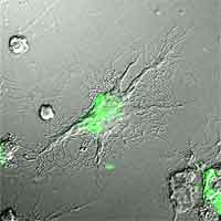
 1,300 to 1,400 grams and several thousand kilometers of about 100 billion interconnected nerve cells control every movement, thought, sensation, and emotion that comprise the human experience. Within the brain and spinal cord there are ten thousand distinct varieties of neurons, trillions of supportive cells, a few more trillion synaptic connections, a hundred known chemical regulating agents, kilometers of minuscule blood vessels, and untold mysteries of how - almost flawlessly - all these components work together. This is the amazing brain. Given the incredible complexity of the brain, it doesn't come as a big surprise that a lot of things can go wrong. The A-Z of brain disorders is a very long list. Several of these disorders (such as Parkinson and Alzheimer disease, but also schizophrenia, epilepsy, and bipolar disorder), not to mention tumors, are so severe that they require treatment of the brain. But even when there are promising pharmaceutical compounds for their treatment, more than 98% of these potential agents do not reach the drug development stage. The reason is the blood-brain barrier (BBB), a tight seal of endothelial cells lines the blood vessels in the brain and acts as a barrier to protect its cells. BBB strictly limits transport into the brain through both physical (tight junctions) and metabolic (enzymes) barriers and keeps most substances, such as chemicals and large biomolecules, out of the brain. The combined use of peptides and nanotechnology offers tremendous hope in the treatment of brain disorders by offering a way for drugs (the therapeutic kind) across the BBB.
Jan 7th, 2008
 The human eye is an amazing organ. It is small, the eyeball itself weighs only about 7 grams, and it is amazingly sensitive. The eye can detect a single photon. The eye can be quicker then a race car - the young human eye can focus from infinity to 7cm in 350 milliseconds - but slow enough to witness a snail crawling across a beach. The eye can capture objects at various different angles, such as birds flying overhead or a person walking right beside you. Because the eye is such a complex optical system, it is not surprising that the list of diseases and infections that can endanger our vision is a long one. One common age-related condition is cataract. Cataract is caused by alterations in the protein structure of the lens which result in light scattering. The lens can then no longer transmit a clear picture to the retina where it can be processed and sent through the optic nerve to the brain. By age 65, over 40% of people have a cataract. Cataract is the most common cause of blindness in the world, although it is treatable. While cataract surgery is the most successful medical procedure, the inability to control penetration of the pharmacological agents into the lens and target specific intracellular biochemical pathways has impeded the success of pharmacological treatment of cataracts. Researchers are now studying the application of nanotechnology to eye lens diseases, in particular for new methods for visualizing and targeting specific intracellular mechanisms within the eye.
Jan 4th, 2008
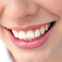 The concept of nanodentistry was introduced by Freitas in 2000: "Nanodentistry will make possible the maintenance of comprehensive oral health by employing nanomaterials, biotechnology including tissue engineering, and, ultimately, dental nanorobotics." Dental nanorobots are certainly many years off but researcher are making progress already with nanotechnology in dental care applications such as composites, bonding agents, and impression materials as well as nanostructured implant materials. For those of you with hypersensitive teeth, a new nanotechnology treatment proposed by researchers in Taiwan might one day bring pain relief. Dentine hypersensitivity (dentin is the main tissue that forms the shape of the tooth; this material exists between the pulp and the enamel, and is comprised of a series of dentinal tubules stacked on top of each other) leads to pain when fluid movement in dentinal tubules (microscopic canals that run from the outside of the dentin to the nerve inside the tooth) promotes mechanical deformation of nerve endings at the pulp/dentine interface, which is transmitted as a painful sensation. Researchers have found that sensitive teeth have an increased number of dentinal tubules (35.6% compared to 9.3%) and are wider in diameter than the dentinal tubules of non sensitive dentine. The Chinese researchers have demonstrated that this tubules can be blocked with the aid of gold nanoparticles. The world's smallest gold fillings, so to speak.
Jan 3rd, 2008
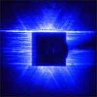 Shorter-wavelength surface-emitting laser sources are important for a variety of fields including photonics, information processing and biology. Researchers in Japan were successful in developing a current-driven blue-violet photonic crystal surface-emitting laser. They developed a fabrication method, named 'air holes retained over growth', in order to construct a two-dimensional gallium nitride/air photonic crystal structure. The resulting periodic structure has a photonic crystal band-edge effect sufficient for the successful operation of a current-injection surface-emitting laser. This represents an important step in the development of laser sources - from both a scientific and engineering point of view - that could be focused to a size much less than the wavelength and be integrated two-dimensionally at such short wavelengths.
Jan 2nd, 2008
 Subscribe to our Nanotechnology Spotlight feed