Showing Spotlights 2353 - 2360 of 2838 in category All (newest first):
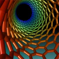 More and more carbon nanotube (CNT) applications are moving from the research lab into commercial products. For example, CNTs can be found already in tennis rackets and bicycles, displays and TV screens, and numerous resins used by aerospace, defense, health care, and electronics companies. Not surprisingly, CNT production is growing by hundreds of metric tons a year. One of the large suppliers alone, Bayer, is talking about having 3,000 metric tons of production capacity in place by 2012. As a result of the increasing supply, prices are dropping fast. While a kilogram of multi-walled CNTs (MWCNTs) sold for tens of thousands of dollars just a few years ago (and single-walled CNTs still do), the price for some types of MWCNTs has fallen to hundreds of dollars per kg. Recent market analyses forecast sales of all nanotubes to reach $1 billion to $2 billion annually within the next four to seven years. In terms of dollar value, electronics devices will be the largest end-use category, although composite materials in automotive applications may account for greater volumes. These volumes are expected to approach several thousand metric tons per year. This means that the exposure to CNTs, especially by factory workers, will increase substantially over the next few years. Since the jury is still out as to the toxicity of nanotubes it appears prudent to at least develop suitable sensor technology to detect CNTs, especially in the workplace.
Feb 4th, 2008
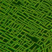 The vision of revolutionary bottom-up nanotechnology is based on a concept of molecular assembly technologies where nanoscale materials and structures self-assemble to microscale structures and finally to macroscopic devices and products. We are a long way from realizing this vision but researchers are busily laying the foundation for nanoscale engineering. Assembling nanoscopic components into macroscopic materials is an appealing goal but one of the enormous difficulties lies in bridging approximately six orders of magnitude that separate the nanoscale from the macroscopic world. Until machinery capable of automated and industrial-scale nano-assembly can be built, the parallelism of chemical synthesis and self-assembly is necessary when controlling materials at the nanoscale. An obvious direct approach to molecular nanotechnology therefore is to start with organic molecules as building blocks. Modest from the viewpoint of molecular manufacturing visionaries, but quite fascinating to a lot of scientists, research into nanofibers, as a modification of organic crystals, is making good progress. New research results coming out of Denmark offer the basis for a novel organic-molecule-based nanotechnological concept that allows for a multitude of applications in fundamental research and in device applications. Essentially, this concept is based on three steps: 1) directed self-assembled surface growth of nanofibers from functionalized molecules; 2) transfer and manipulation of individual fibers as well as of ordered arrays; and 3) device integration.
Feb 1st, 2008
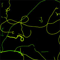 'Smart' is the key buzz word used by materials engineers when they describe the future of coatings, textiles, building structures, vehicles and just any material that you can think of. Materials are made 'smart' when they are engineered to have properties that change in a controlled manner under the influence of external stimuli such as mechanical stress, temperature, humidity, electric charge, magnetic fields etc. Nature of course is full with 'smart' materials that are capable of adapting to new tasks, are self-healing, and can self-assemble autonomously simply out of a solution of building blocks. Duplicating this feat with man-made materials will one day become a reality thanks to nanotechnology. Scientists not only dream about self-repairing cars or building walls that turn transparent like windows, they are actively working on the first steps towards these goals. Simple smart materials (that are not nanotechnology based) are already a reality, such as piezoelectric materials and shape memory alloys. Emerging nanotechnologies are now about to give scientists the tools to take smart materials to the next performance level. For instance, the European project Inteltex is developing a new, multifunctional textile that could be used as a wallpaper to detect temperature changes or chemical leakage or that could be used in medical and protective wear to monitor body temperature and mechanical stress. MIT's Institute for Soldier Nanotechnologies works on smart surfaces that switch properties. Nanotechnology-enabled smart materials are still very early days but basic progress is being made. Another small building block towards smart materials was recently reported by Italian researchers who demonstrated photo-switchable nanofibers based on the reversible transformation between two molecular photochemical states, exhibiting different chemico-physical characteristics.
Jan 31st, 2008
 Our sense of touch connects us to the world around us and is an integral part of how we experience things, both physically and emotionally. In the virtual world of remote-control robots, scientific models or computer games, users generally lack tactile, or haptic (from the Greek word Haphe, pertaining to the sense of touch), feedback, which either makes delicate manipulative tasks difficult or keeps the subject purely visual and often inscrutable (an electron microscope image of a nanoscale object, for instance). The desire for natural and intuitive human machine interaction has led to the inclusion of haptics in man-machine interfaces. The user is able to control inputs to the system through hand movements and in turn receives feedback through tactile stimulation in the hands. Sophisticated, state-of-the-art haptic user-interface software is capable of adding interactive, realistic virtual touch capabilities to human-computer interactions. Among the uses are medical applications, remote vehicle or robotic control, military applications, and video games. Users are said to feel realistic weight, shape, texture, dimension, dynamics, and force effects. Applying the use of real-time virtual reality and multisensory user interface to nanoscience, scientists in France have begun to open up the otherwise only scientifically described reality of the nanoworld to a non-scientific public.
Jan 30th, 2008
 When the U.S. enacted its 21st Century Nanotechnology Research and Development Act in 2003 it was clearly understood that the impact of nanotechnologies on all aspects of society would be deeply transformational. As the National Nanotechnology Initiative was set up, its goals were not only defined as 'maintaining a world-class research and development program aimed at realizing the full potential of nanotechnology' but also to 'facilitate transfer of new technologies into products for economic growth, jobs, and other public benefit'. The first part regarding world-class R&D is happening. The second part, converting the research and development results into economic growth and jobs, is nowhere to be seen yet.
Jan 29th, 2008
 The World Economic Forum, whose 2008 Annual Meeting ended on Sunday, has founded the Global Risk Network in 2004 in response to concern that the international community and the global business community were not yet able to respond adequately to a changing global risk landscape. The Program has moved forward in partnership with Citigroup, Marsh & McLennan Companies, Merrill Lynch, Swiss Re and the Center for Risk Management and Decision Processes, and Wharton School. In an increasingly complex and interconnected global environment, risks can no longer be contained within geographical or system boundaries. No one company, industry or state can successfully understand and mitigate global risks. The World Economic Forum, with numerous links to business networks, policy-makers and government, NGOs and think-tanks, is in a unique position to advance new thinking on global risks, to generate risk mitigation measures and to integrate current knowledge on global risks. Over the past few years, the Global Risk Network team has released an annual report. This years' report 'Global Risks 2008' was published two weeks ago. In it, as in previous years, nanotechnology was characterized as a global core risk.
Jan 28th, 2008
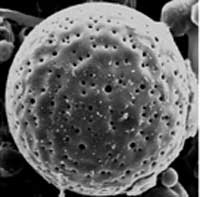 Hollow polymeric micro- and nanoparticles have numerous existing and many anticipated applications in drug delivery, ranging from the controlled release of drugs, cosmetics, inks, pigments or chemical reagents to the protection of biologically active species, and removal of pollutants. Encapsulation also allows drug targeting via cell and tissue-specific ligands. There is a variety of methods available for synthesis of polymer microspheres with hollow interiors. The hollow particles are most commonly prepared by coating the surfaces of colloidal templates with thin layers of the desired material (or its precursor), followed by selective removal of the templates by means of calcination or chemical etching. For polymers, methods such as emulsion polymerization, phase separation, cross-linking of micelles and self-assembly have also been demonstrated for generating hollow structures. The hollow polymer particles produced by these methods present either a closed-core-shell structure or many small pores on their surface. However, these synthetic approaches present limitations on the choice of polymers that can be produced as hollow microspheres. Also, the number, size and shape of the surface pores can not be easily manipulated. When these materials are used for encapsulation-related applications, the encapsulation of the desired functional materials is usually too slow and/or too labor-intense. These problems have motivated scientists to develop the synthesis of a new class of polymer microspheres, which they called microscale fish bowls. Their unique feature consists in the presence of one big pore on their surface that allows easy and fast diffusion of a functional material to be encapsulated. Another new feature is that this newly developed method presents no limitations on the choice of polymers that can be produced as microscale fish bowls.
Jan 25th, 2008
 Sophisticated optical lithography techniques have been developed by the semiconductor industry to pack more and more transistors onto chips. On the road to a billion transistors per chip, Intel has already developed transistors so small that 200 million of them could fit on the head of a pin. As if that wasn't small enough, scientists are pushing further down, hoping to be able one day to reliably (and affordably) control surface features as small as 1 nm. With today's technology, cost-effective fabrication in the sub-50 nm range is a major challenge. Given the advanced development of (nano)lithography it is not surprising that various forms of it are the most common techniques used by nanotechnology researchers for manipulating sub-100 nm surface features. With the current state of optical lithography it appears that traditional commercial lithography techniques will not be cost effective below 30 nm. State-of-the-art electron beam lithography (EBL) has been proved to be capable of delivering resolution in the 10 nm range. Unfortunately, EBL is slow, very expensive and it is very unlikely that it can effectively go below 10 nm. The same limitations hold for x-rays and focused ion beams (FIBs), with additional tremendous difficulties in developing equipment for beam manipulation and focusing on nanometer scales.
Jan 24th, 2008
 Subscribe to our Nanotechnology Spotlight feed