Showing Spotlights 2337 - 2344 of 2838 in category All (newest first):
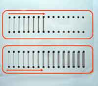 Transparent electrical conductors pervade modern electronic devices, providing a critical component of digital cameras and video recorders, solar cells, lasers, optical communication devices, and solid-state lighting. Given the advantageous electrical properties of carbon nanotubes (CNTs), researchers already have used CNTs to impart electrical conductivity to polymeric thin films and coatings while maintaining excellent optical transparency. While this was done initially with complex lithography processes and sophisticated deposition facilities, advances in nanotube chemistry have enabled both the dissolution and dispersion of CNTs in various solvents. This has led to new alternatives for fabricating CNT patterns by simply dispensing/printing the dissolved/dispersed particles on substrates. Most methods of fabricating CNT transparent conductive film, such as vacuum filtering, laser printing, dip coating, spray coating and contact printing, require two fabrication steps to achieve the patterns. The first is to fabricate the film over all the area of the substrate. The second is to make the pattern by chemical etching or pattern transfer. In contrast, a direct printing approach has the merits of forgoing complex and expensive equipment, reducing the fabrication processes, saving the amount of material used, and removing chemical exposure in the processes. The use of off-the-shelf inkjet printers for printing patterns of carbon nanotubes on paper and plastic surfaces has been previously reported. These first inkjet demonstrations were done with multi-walled CNTs but now researchers in South Korea have managed to print pure single-walled CNTs based inkjet patterns.
Feb 26th, 2008
 Adhesive tapes are ubiquitous in our lives, whether it's on the back of a yellow sticky note, the tape that closes baby diapers, masking connectors on printed circuit boards, or surgical tape in hospitals. Most adhesive tape will stick to a wide variety of surfaces - provided that they are clean and dry. Adhesive tapes are made up of two components: a carrier which is usually paper or plastic, and an adhesive which is either water or solvent based. Many modern adhesive tapes use pressure sensitive adhesives. When you apply pressure to the tape with your finger, a strong adhesive bond is formed. Most tapes have poor ageing properties and will deteriorate quickly: with time, after several uses, or as the sticky side becomes dirty, they lose their adhesive ability. As we have reported previously, scientists are very interested in exploring the secret of the gecko's adhesive properties and to use this knowledge to create superior man-made adhesives. But it's not just the stickiness that intrigues researchers: because geckos are able to walk across a dusty or dirty surface and then scale a vertical wall without problems, their feet must also possess some kind of self-cleaning ability. Scientists have now managed to mimic the remarkable self-cleaning abilities of the gecko, as well as lotus leaves, and incorporate this ability into the design of a self-cleaning, carbon nanotube based adhesive material.
Feb 25th, 2008
 Only 30% of all freshwater on the planet is not locked up in ice caps or glaciers (not for much longer, though). Of that, some 20% is in areas too remote for humans to access and of the remaining 80% about three-quarters comes at the wrong time and place - in monsoons and floods - and is not always captured for use by people. The remainder is less than 0.08 of 1% of the total water on the planet. Expressed another way, if all the earth's freshwater were stored in a 5-liter container, available fresh water would not quite fill a teaspoon. The problem is that we don't manage this teaspoon very well. Currently, 600 million people face water scarcity. Depending on future rates of population growth, between 2.7 billion and 3.2 billion people may be living in either water-scarce or water-stressed conditions by 2025. Freshwater looks like it will become the oil of the 21st century - scarce, expensive and the reason for armed conflicts. While in our previous article we have only talked about nanotechnology and water in general terms, a new paper gives us the opportunity to look in more detail at the role that nanotechnology could play in resolving issues relating to water shortage and water quality. This review highlights the uses of nanotechnology in areas relevant to water purification, including separation and reactive media for water filtration, as well as nanomaterials and nanoparticles for use in water bioremediation and disinfection.
Feb 22nd, 2008
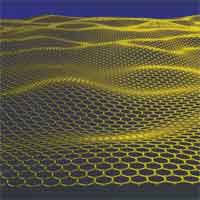 There has been quite a buzz about graphene, a single atomic layer thick, plane of carbon atoms arranged in a honeycomb lattice. Discovered only in 2004, graphene exhibits many exotic properties and currently is considered the most exciting new material system among nanotechnology researchers. This rising star in material science exhibits remarkable electronic properties that qualify it for applications in future optoelectronic devices. In a first experimental study of the thermal conductivity of single-layer graphene, researchers found that on top of many unique electronic properties, graphene also is an extraordinary good heat conductor. Measurements revealed that graphene's near room temperature thermal conductivity, which is in the range from 3500-5300 W/mK, is much higher than that of diamond, the best bulk crystal heat conductor. It appears that the thermal conductivity of graphene is larger than conventionally accepted experimental values reported for individual suspended carbon nanotubes (CNTs) and corresponds to the upper bound of the highest values reported for single-wall CNT bundles. The superb thermal conduction property of graphene is beneficial for its proposed electronic applications and establishes graphene as an excellent material for thermal management also in optoelectronics, photonics and bioengineering.
Feb 21st, 2008
 A number of researchers and organizations such as the Meridian Institute in the US believe that nanotechnology could contribute to some or all of the UN Millennium Development Goals, aiming for poverty reduction by 2015. Applications of nanotechnology that could benefit those living in poverty include diagnostics and therapies for infectious diseases, water purification and desalination, sustainable energy production, and environmental monitoring and remediation. Nanotechnology could also contribute to food security by boosting the yields of food crops, and packaging materials coated with nanoparticles that will allow food to be stored longer. So far, nanotechnology has been an area of 'technology push', with substantial investments in both generic research and technology development, in the absence of clear market demand. Worldwide, private investments in research have recently overtaken public funding, but the potential advantages of nanotechnology-based products compared to other alternatives are not yet clear. Also, there is a growing global debate on the ethical, legal and social aspects of nanotechnology, in particular the potential risks to human health and the environment posed by engineered nanomaterials. Nanotechnology is still mainly a solution looking for problems to solve, including sustainable development issues.
Feb 20th, 2008
 The list of great monuments and frescoes destroyed or seriously damaged by negligence or criminal action is dramatically increasing, and the biggest culprit is air pollution. Pollutants such as sulfur dioxide and nitrogen oxides are the most serious causes of degradation in carbonate stone, which in the form of marble, limestone and similar materials comprises some of the most important monuments and artifacts in the world. The main damage to monuments is that the stonework becomes sulphated through the transformation of calcium carbonate to calcium sulphate owing to the presence of sulphur dioxide. Two forms of deterioration then take place: the constitution of a black film in areas sheltered from the rain, and elsewhere the crumbling of the interior of the stone. For instance, UNESCO estimates that the surface eaten away annually in a cultural heritage site such as Venice represents 6 per cent of marble and stone monuments and 5 per cent of frescoes. The problem is not only what causes the damage but also how repairs are done. Quite often, the experts in charge of restoration work - architects, restorers, renovators - conduct their work without previous scientific studies of the damaged monument. Specifically the consolidation of decayed stone in historical buildings is a common intervention that can cause irreparable damage to the monument. Although commercial products, such as alkoxysilanes that are commonly used to consolidate stone, present unquestionable advantages they also present certain disadvantages totally ignored by the experts in charge of their application. Scientists in Spain are committed to the development of new nanotechnology materials specifically suited to stone-based historical structures. Their objective has been the development of a new nanomaterial which forms a crack-free gel in the pores of the treated stone.
Feb 19th, 2008
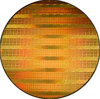 Due to their exceptional electronic and mechanical properties, as well as their nanoscale size, carbon nanotubes (CNTs) could become the active electronic elements in addressing next generation electronic requirements for which silicon is not a solution. Already, it has been shown extensively that semiconducting CNTs can be made into electronic components such as transistors and switches. Their thermal, mechanical, chemical stability, and large current-carrying capacity make CNTs attractive for applications not only in in electrical interconnects but also field-effect transistors, cold cathode field emitters, and sensors. Some of the problems in developing CNT-based electronic devices have to do with building reliable interconnections between CNTs and external electrical and mechanical systems and in developing a reliable fabrication batch process to allow for industrial-scale mass production that supports the direct manipulation and placement/growth of CNTs at specific locations. Pointing to a possible solution, researchers now have demonstrated controllable and simultaneous wafer-scale assembly of CNT networks by dielectrophoresis.
Feb 18th, 2008
 Carbon nanotubes (CNTs) have shown promise as an important new class of multifunctional building blocks and innovative tools in a large variety of nanotechnology applications, ranging from nanocomposite materials through nanoelectronics to biomedical applications. The exploration of CNTs in biomedical applications is well underway and exploratory uses have included CNT-coated implants, drug delivery and CNTs as components of biosensors. Notwithstanding the still not satisfactorily addressed issue of toxicity, CNTs' properties such as high strength, high electrical and thermal conductivities, and high specific surface area render them particularly useful in the fabrication of nanocomposite-derived biomedical devices. In one particular area - biomaterials applied to bone - CNTs are anticipated to improve the overall mechanical properties for applications such as high-strength arthroplasty prostheses expected to remain in the body for a long time, or fixation plates and screws that will not fail or impede healing of bone. In addition, CNTs are expected to be of use as local drug delivery systems or scaffolds to promote and guide bone tissue regeneration. A new study by Japanese scientists clearly demonstrates that multi-walled CNTs (MWCNTs) have good bone-tissue compatibility, permitting bone repair and becoming closely integrated with bone tissue. Furthermore, under certain circumstances, their results indicate that MWCNTs accelerate bone formation.
Feb 15th, 2008
 Subscribe to our Nanotechnology Spotlight feed