Showing Spotlights 2313 - 2320 of 2838 in category All (newest first):
 The most common type of modern transistor, and the type of transistor used in integrated circuits, is called a field-effect transistor (FET). The FET is so named because it relies on an electric field to control the shape and hence the conductivity of a 'channel' (the charge carrier) in a semiconductor material. This field causes a second electrical current to flow across the semiconductor, identical to the first weak signal, but stronger. Since the invention of the first transistor in 1947, the vast majority of electronic devices have been based on inorganic semiconductors, which in most cases has been silicon. Due to the demand for lightweight, flexible opto-electronic devices such as displays, solar cells and lasers, organic materials have become an important new class of semiconductor as they combine the virtues of plastics, which can be easily shaped, with those of semiconductors which are the basis of all microelectronics. Organic field-effect transistors (OFETs) have been mainly based on two types of semiconductors: conjugated polymers and small conjugated molecules. A recent review, published in Chemical Society Reviews, provides a general introduction about the current standing in the area of OFETs focusing on the new processable small molecules that have been recently reported for their use as organic semiconductors.
Apr 2nd, 2008
 The newly created U.S. Nanotechnology Protection Agency (NPA) announced today, April 1, 2008, that, effective immediately, all laboratories and production facilities for molecular assemblers (commonly called nanobots) need a special license and have to follow strict guidelines in all research and production facilities that deal with nanoassemblers. At the same time, the NPA declared gray goo a hazardous substance. While the NPA regulations will have an immediate economic impact on many nanotechnology companies, most have been preparing for this dreaded day. However, public and media reactions seem to indicate that the public and many organizations were taken completely by surprise.
Apr 1st, 2008
 You probably have seen quite a number of research reports on the amazing climbing abilities of geckos. Here at Nanowerk, we ran several Spotlights on this topic, for instance on mimicking gecko toe structures to fabricate super-strong dry adhesives. One demonstration of so-called 'gecko tape' has already been used in building Stickybot, a quadruped robot capable of climbing smooth vertical surfaces, such as glass, acrylic and whiteboard. In addition to the animal kingdom, scientists have started looking at plants to identify biological climbing mechanisms that could be exploited for engineering applications. One obvious candidate is ivy, a climbing woody plant. Researchers now have found that ivy secretes nanoparticles which allow the plant to affix to a surface and play an important role in the plant's climbing capability. This ivy secretion mechanism may inspire new, 'green' methods for synthesizing nanoparticles biologically or new approaches to adhesion mechanisms for mechanical devices.
Mar 31st, 2008
 An Interagency Working Group on Manufacturing Research and Development established by the National Science and Technology Council has identified three technology areas as key research and development priorities for future manufacturing: Manufacturing for Hydrogen Technologies; Nanomanufacturing; and Intelligent and Integrated Manufacturing. The Working Group summarized their findings in a new report titled 'Manufacturing the Future.' Although this report is specific to the U.S., most of its general conclusions and recommendations apply to most other industrialized nations and their industrial nanotechnology efforts as well. Nanotechnology is viewed throughout the world as a critical driver of future economic growth and as a means to addressing some of humanity's most vexing challenges. Because of its broad range of prospective uses, nanotechnology has the potential to impact virtually every industry, from aerospace and energy to healthcare and agriculture. Nanomanufacturing integrates science and engineering knowledge and develops new processes and systems to assure quality nanomaterials, to control the assembly of molecular-scale elements, and to predictably incorporate nanoscale elements into nano-, micro-, and macroscale products utilizing new design methods and tools. Efforts in this area are directed toward enabling the mass production of reliable and affordable nanoscale materials, structures, devices, and systems. Nanomanufacturing includes the integration of ultra-miniaturized top-down processes and evolving bottom-up or self-assembly processes.
Mar 28th, 2008
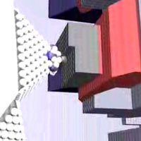
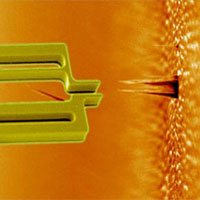
 A key challenge in nano-optics is to bring light to and collect light from nano-scale systems. In conventional electronics, the interconnect between locally stored and radiated signals, for example radio broadcasts, is formed by antennas. For an antenna to work at the wavelength of light it needs to be greatly scaled down, to the nanoscale. Antennas play a key role in our modern wireless society. The electromagnetic waves sent and received by antennas are the messages that enable communication between electronics. Antennas with a wide variety of sizes make it possible for us receive radio broadcasts, watch television and talk to others on a mobile phone. For an effective communication, the antenna needs to direct signals towards their intended target and, vice versa, collect signals from a desired source. Now, researchers have shown that the concept of an antenna is equally well applied to direct the visible light sent out by a single molecule. For an antenna to work with visible light, it needs to be millions of times smaller than a conventional antenna. In this case, it is only 80 nanometer long. By placing the antenna near an individual molecule the light from that molecule is re-directed; the molecular message can be steered to a desired target, making efficient communication possible.
Mar 27th, 2008
 The success of the computer and communications industry is mainly due to the possibility of a large volume and low cost production output: silicon wafers containing myriad micro and nano structures are at the basis of Complementary Metal Oxide Semiconductor (CMOS) technology. A challenge is the realization of spatially ordered nanostructures in silicon that have many interesting applications like photonic crystals to mod the flow of light, chemical sensors, devices to alter the wetting of liquids on a surface, and as capacitors in high-frequency electronics used in mobile phones. The incorporation of such structures on existing silicon chips is greatly desired, and adapting conventional semiconductor nanofabrication to that end is widely pursued. Just a few days ago we wrote about the general aspects and challenges of silicon photonics and today we are taking a look at a specific fabrication challenge. The challenge for researchers is to to obtain photonic crystals with stop bands in the telecommunication wavelength regions, i.e.1330 nm and 1550 nm. To do that, the diameter of these pores must be smaller than 500 nm. The pore to pore distances, also referred to as pitch or interpore distance, must be well below 1 micrometer. Furthermore the depth to diameter aspect ratio of the pores must be as high as possible to obtain photonic crystals with large enough volumes. Researchers in The Netherlands now have demonstrated a method to etch arrays of nanopores in silicon with record depth-to-diameter ratios. These structures are suitable for nanophotonics and were made completely with CMOS compatible technologies, making integration of photonic structures in silicon chips feasible.
Mar 26th, 2008
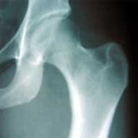 Polymethylmethacrylate (PMMA), a clear plastic, is a pretty versatile material. Plexiglas windows are made from PMMA. Acrylic paints contain PMMA. It also remains one of the most enduring materials in orthopedic surgery where it has a central role in the success of total joint replacement. Being part of a group of medical materials called 'bone cement', its use includes the fixation of biomaterials such as artificial joints to bone, the filling of bone defects and, also, as a drug-delivery system. Beginning in the 1970s, many successful results have been reported for total hip replacement using PMMA cement; however, failures of fixation have also occurred. The fixation strength of PMMA cement to bone is mainly dependent on mechanical interlocking, but it is known that a fibrous tissue layer intervenes between cement and bone - PMMA cement never bonds directly to the bone. One of the problems associated with the conventional types of bone cement used is their unsatisfactory mechanical and exothermic reaction properties. Other problems with PMMA cement include the biological response, leakage of the monomer of methylmethacrylate and a high curing temperature, which can damage cell activity. Ideally, a bone cement material must functionally match the mechanical behavior of the tissue to be replaced, it must be able to form a stable interface with the surrounding natural tissue and be effective in guided tissue regenerative procedures, it should be easy to handle, biologically compatible, non-supporting of microbial growth, and non-allergenic. A novel nanocomposite of carbon-nanotube-reinforced PMMA/HA is a demonstration of how nanomaterials will play an increasing role in the synthesis of next-generation biomedical applications.
Mar 25th, 2008
 In our Nanowerk Spotlights we usually stay with both feet firmly on the grounds of science and shy away from the science fiction and sensationalist aspects of nanotechnology. So today's headline might come as a surprise to you (but just to be safe we put a question mark in). Of course, there are no nanobots yet, and won't be for a while, but one of the fundamental problems to be solved for possible future molecular machinery is the challenge of controlling many molecule-sized machines simultaneously to perform a desired task. Simple nanoscale motors have been realized over the past few years but these are systems that do nothing more than generate physical motion of their components at a nanoscale level. To build a true nanorobot - a completely self-contained electronic, electric, or mechanical device to do such activities as manufacturing at the nanoscale - many breakthrough advances will need to be achieved. One of them is the issue of controlling large numbers of devices, i.e. how to build and program the 'brains' of these machines. Another issue is to separate the concept of science fiction style 'thinking' robots (artificial intelligence) from a more realistic (yet still distant) concept of machines that can be programmed to perform a limited task in a more or less autonomous way for a period of time. These tasks could range from fabricating nanoscale components to performing medical procedures inside the body. For nanoscale machinery this would require the availability of nanoscale control units, i.e. computers. Researchers in Japan are now reporting a self organizing 16-bit parallel processing molecular assembly that brings us a step closer to building such a nanoscale processor.
Mar 20th, 2008
 Subscribe to our Nanotechnology Spotlight feed