Showing Spotlights 1993 - 2000 of 2855 in category All (newest first):
 As a reader of Nanowerk we would like to invite you to joins us at the MicroNanoTec trade show at HANNOVER MESSE 2010 completely free of charge. HANNOVER MESSE will embrace microsystems technology and nanotechnology in a single trade fair under the new name MicroNanoTec. Microsystems technology and nanotechnologies have formed an important part of HANNOVER MESSE for many years. In the past they have mainly been presented at the leading trade fair MicroTechnology. The change of name signals a further expansion of microtechnology and nanotechnology at HANNOVER MESSE. The world's leading showcase for industrial technology is staged annually in Hannover, Germany. The next HANNOVER MESSE will be held from 19 to 23 April 2010.
Dec 3rd, 2009
 Chip structures already have reached nanoscale dimensions but as they continue to shrink below the 20 nanometer mark, ever more complex challenges arise and scaling appears not to be economically feasible any more. And below 10 nm, the fundamental physical limits of CMOS technology will be reached.
One promising material that could enable the chip industry to move beyond the current CMOS technology is graphene, a monolayer sheet of carbon. Notwithstanding the intense research interest, large scale production of single layer graphene remains a significant challenge. Researchers at Cornell University have now reported a new technique for producing large scale single layer graphene sheets and fabricating transistor arrays with uniform electrical properties directly on the device substrate.
Chip structures already have reached nanoscale dimensions but as they continue to shrink below the 20 nanometer mark, ever more complex challenges arise and scaling appears not to be economically feasible any more. And below 10 nm, the fundamental physical limits of CMOS technology will be reached.
One promising material that could enable the chip industry to move beyond the current CMOS technology is graphene, a monolayer sheet of carbon. Notwithstanding the intense research interest, large scale production of single layer graphene remains a significant challenge. Researchers at Cornell University have now reported a new technique for producing large scale single layer graphene sheets and fabricating transistor arrays with uniform electrical properties directly on the device substrate.
Dec 2nd, 2009
 Metastasis is caused by marauding tumor cells that break off from the primary tumor site and ride in the bloodstream to set up colonies in other parts of the body. These breakaway cancer cells in the peripheral blood are known as circulating tumor cells (CTCs). Detecting and analyzing these cells can provide critical information for managing the spread of cancer and monitoring the effectiveness of therapies. Nanotechnology researchers have now developed a an efficient cell-capture platform based on 3D nanostructured substrates. The device is engineered out of nanoscale silicon pillars and has managed to capture up to 65 percent of circulating tumor cells in lab samples within human blood - far more than any existing diagnosis tool for CTC capture.
Nov 30th, 2009
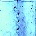 A lot of the scientific knowledge in chemistry and biology comes from experiments on ensembles of molecules by which a vast number of duplicate behaviors are investigated and averaged responses are recorded. Especially the ability to make measurements at the single molecule level provides crucial information about biological and chemical systems. This research depends on molecular manipulation technologies that are able to isolate individual molecules and sequentially transport them for measurement and, potentially, manipulation. To this end, generation and manipulation of small, highly monodisperse droplets have received a lot of attention in the biotech community recently. Using a simple droplet generator chip, scientists can generate millions of droplets in a short amount of time. Each individual droplet is isolated from another droplet, hence, meaning that a million droplets constitute a million individual microreactors running a million reactions simultaneously.
Nov 25th, 2009
 Single molecule detection requires tools that have the detection sensitivity at the scale of single molecules. This could mean a spatial resolution requirement of only a few nanometers especially if the precise location of the molecule needs to be mapped. Researchers have already developed spectroscopic techniques capable of physical and chemical mapping on a nanometer scale. Researchers in Italy have now reported the design, fabrication and application of a photonic-plasmonic device that is fully compatible with atomic force microscopy and Raman spectroscopy - an approach that is novel in both scientific and technological aspects. The device consists of a two-dimensional dielectric photonic crystal cavity patterned on an AFM cantilever, together with a tapered silver waveguide placed at the center of the cavity.
Nov 24th, 2009
 OLEDs - organic light-emitting diodes - are full of promise for a range of practical applications. With more efficient and cheaper OLED technologies it becomes possible to make ultraflat, very bright and power-saving OLED televisions, windows that could be used as light source at night, and large-scale organic solar cells. One of the drawbacks of this technology, apart from its currently high manufacturing cost, are problems with the OLED fabrication process where issues such as material damage, yield, and thickness uniformity haven't been completely solved yet. Researchers in Japan have now proposed a nanoparticle-based deposition method that might be able to overcome these fabrication problems.
Nov 23rd, 2009
 Europe is a key player in nanotechnology and, about on the same level as the U.S., invests hundreds of millions of dollars, or rather euros, into nanotechnology research and development projects. Whereas the U.S. National Nanotechnology Initiative (NNI) in was established in 2001 to coordinate Federal nanotechnology research and development, the European Union's slowly grinding bureaucratic mills came up with a comparable program only three years later. In May 2004, the European Commission adopted the Communication Towards a European Strategy for Nanotechnology. It seeks to bring the discussion on nanoscience and nanotechnology to an institutional level and proposes an integrated and responsible strategy for Europe. Since then, the EU has issued updates on how they are doing with two implementation reports, the last one issued just a few days ago.
Nov 19th, 2009
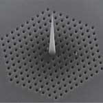
 Many of today's high-tech products rely on nano-level functional structures, and in products such as mobile phones, integrated circuits and glasses they have already become commonplace. But with increasing demands on products and their quality, tiny structures and the ability to evaluate them are also becoming decisive factors for the production of everyday products. The experience of a ball-point pen maker shows how atomic force microscopy enables highly accurate quality control during manufacturing, eliminating entire production steps in the process. Everyone has had to contend with scratchy or messy ball-point pens, but not everyone knows that often this malfunction is the result of a manufacturing error: smooth writing depends largely on the roughness of the sphere at the tip of the pen. Its roughness needs to lie in a well-defined interval: too rough, and the pen leaks; too smooth, and it scratches and fails to transport enough ink. The roughness of this little sphere thus becomes the decisive quality indicator of the entire writing apparatus.
Nov 18th, 2009
 Subscribe to our Nanotechnology Spotlight feed