Showing Spotlights 1961 - 1968 of 2855 in category All (newest first):
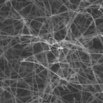
 Materials engineers are keen to exploit the outstanding mechanical properties of carbon nanotubes for applications in fibers, composites, fabrics and other larger-scale structures and devices. The ability to fabricate continuous, multifunctional yarns represents an important step in this direction. The development of a continuous, weavable multilayered CNT yarn with superior mechanical, structural, surface, and electrical properties would open the way for a wide range of structural and functional applications, including composites, intelligent fabrics, catalyst supports, and sensors. Researchers in China now demonstrate the fabrication of a novel continuous yarn of CNTs with a multiple-layer structure by a CVD spinning process. The yarn consists of multiple monolayers of CNTs concentrically assembled in seamless tubules along the yarn axis.
Feb 9th, 2010
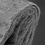
 Carbon nanotubes are 'strange' nanostructures in a sense that they have both high mechanical strength and extreme flexibility. Deforming a carbon nanotube into any shape would not easily break the structure, and it recovers to original morphology in perfect manner. Researchers in China are exploiting this phenomenon by making CNT sponges consisting of a large amount of interconnected nanotubes, thus showing a combination of useful properties such as high porosity, super elasticity, robustness, and little weight. The nanotube sponges not only show exciting properties as a porous material but they also are very promising to be used practically in a short time. The production method is simple and scalable, the cost is low, and the sponges can find immediate use in many fields related to water purification.
Feb 8th, 2010
 Bismuth telluride and its alloys are unique materials. They are the best thermoelectric materials known today, and they are as important to the thermoelectric industry - for cooling and energy generation applications - as silicon is important to the electronic industry. It has been predicted theoretically that structuring bismuth telluride into crystalline ultra-thin films (with the thickness of few nanometers) would lead to a drastic improvement of the thermoelectric figure of merit, which defines the efficiency of the thermoelectric energy conversion. The improvement comes as a result of the strong quantum confinement of charge carriers and reduction of the thermal conductivity. In addition to their thermoelectric applications, bismuth telluride thin films recently attracted attention as promising topological insulators - a newly discovered class of materials with unusual properties. Researchers have now succeeded in 'graphene-inspired' mechanical exfoliation of atomically-thin crystals of bismuth telluride.
Feb 5th, 2010
 Materials that can produce electricity are at the core of piezoelectric research and the vision of self-powering machines and devices. Nanotechnology researchers are even pursuing nanopiezotronics devices that have the potential of converting biological mechanical energy, acoustic/ultrasonic vibration energy, and biofluid hydraulic energy into electricity, demonstrating a new pathway for self-powering of wireless nanodevices and nanosystems. In addition to miniaturizing piezoelectric devices down to the nanoscale, nanotechnology is also contributing to making next-generation devices more effective. Piezoelectric ceramics for instance generate electrical charge or voltage when they experience stress/strain, and thus are highly efficient at converting mechanical energy into electrical energy. However, ceramics are rigid, which greatly limits the applicability of the energy harvesting. Researchers have now demonstrated that high performance piezoelectric ceramics can be transferred in a scalable process onto rubber or plastic, rendering them flexible without any sacrifice in energy conversion efficiency.
Feb 3rd, 2010
 Multifunctional nanoparticles are at the core of a growing field called theranostics that develops technologies physicians can use to diagnose and treat diseases in a single procedure. The major promise of theranostics is to bring together key stages of a medical treatment, such as the diagnosis and therapy, and thus to make a treatment shorter, safer and more efficient. Theranostic approaches require adequate tools with a high multi-functionality and selectivity. The initial phase of the development of theranostics has already revealed the two general challenges: lack of multifunctional methods and agents, and the lack of selectivity and specificity of available agents - that ultimately requires cell and molecular levels. Researchers have now developed a novel method based on gold nanoparticle-generated transient photothermal vapor nanobubbles, a structure they refer to as plasmonic nanobubbles.
Feb 1st, 2010
 About two years ago we reported on the concept of a biological nanofactory that comprises multiple functional modules: a targeting module specifically targets cells; a sensing module senses and transports raw materials that are present in their vicinity; a biosynthesis module converts raw materials to useful molecules, transport them back to the cell surface, and self-destructs upon completion of this sequence (self-destruct module).
Scientists at the University of Maryland have now demonstrated what was conceptualized in this earlier vision. Moreover they have added a quality that was not originally conceived - the nanofactory needs to have modalities that enable its own assembly. The scientists used the principles of synthetic biology to create the enzyme pathway that has as a part of it an assembly domain. Then, they used 'biofabrication' to assemble antibodies on to the synthesis domain, which enables targeting.
About two years ago we reported on the concept of a biological nanofactory that comprises multiple functional modules: a targeting module specifically targets cells; a sensing module senses and transports raw materials that are present in their vicinity; a biosynthesis module converts raw materials to useful molecules, transport them back to the cell surface, and self-destructs upon completion of this sequence (self-destruct module).
Scientists at the University of Maryland have now demonstrated what was conceptualized in this earlier vision. Moreover they have added a quality that was not originally conceived - the nanofactory needs to have modalities that enable its own assembly. The scientists used the principles of synthetic biology to create the enzyme pathway that has as a part of it an assembly domain. Then, they used 'biofabrication' to assemble antibodies on to the synthesis domain, which enables targeting.
Jan 29th, 2010
 With all the buzz that is being created by portable e-book readers, it's worth taking a look at one of the advanced display technologies - also often referred to as electronic paper - that make these devices happen. Unlike a conventional flat panel display, which uses a power-consuming backlight to illuminate its pixels, electronic paper reflects light like ordinary paper and is capable of holding text and images indefinitely without drawing electricity, while allowing the image to be changed later. Because they can be produced on thin, flexible substrates an due to their paper-like appearance, electrophoretic displays are considered prime examples of the electronic paper category. Electrophoretic displays already are in commercial use, for instance in the Kindle or in the Sony Reader, but so far the displays are mostly black and white. There are still cost and quality issues with color displays. New work by researchers in South Korea shows that organic ink nanoparticles could provide an improved electronic ink fabrication technology resulting in e-paper with high brightness, good contrast ratio, and lower manufacturing cost.
Jan 27th, 2010
 Scientists have great expectations that nanotechnologies will bring them closer to the goal of creating computer systems that can simulate and emulate the brain's abilities for sensation, perception, action, interaction and cognition while rivaling its low power consumption and compact size. DARPA for instance has a program called SyNAPSE that is trying to develop electronic neuromorphic machine technology that scales to biological levels. Started in late 2008 and funded with $4.9 million, the goal of the initial phase of the SyNAPSE project is to 'develop nanometer scale electronic synaptic components capable of adapting the connection strength between two neurons in a manner analogous to that seen in biological systems, as well as, simulate the utility of these synaptic components in core microcircuits that support the overall system architecture.' Independent from this military-inspired research, nanotechnology researchers in France have developed a hybrid nanoparticle-organic transistor that can mimic the main functionalities of a synapse. This organic transistor, based on pentacene and gold nanoparticles and termed NOMFET (Nanoparticle Organic Memory Field-Effect Transistor), has opened the way to new generations of neuro-inspired computers, capable of responding in a manner similar to the nervous system.
Jan 25th, 2010
 Subscribe to our Nanotechnology Spotlight feed