Showing Spotlights 209 - 216 of 237 in category All (newest first):
 Every few months you can read about a recall of food items, be it fresh spinach of bottled infant formula, due to contamination with salmonella, E. coli or some other foodborne pathogen. A pathogen is a an organism that causes disease in another organism. The Centers for Disease Control and Prevention (CDC) estimates that foodborne diseases cause 76 million illnesses, 325,000 hospitalizations, and 5,000 deaths each year. In 2000, the U.S. Department of Agriculture (USDA) estimated the costs associated with five major bacterial foodborne pathogens to be $6.9 billion. The Food and Drug Administration's 2005 Food Code states that the estimated cost of foodborne illness is $10-$83 billion annually. These staggering numbers, not to mention the potential of foodborne pathogens for terrorists attacks, are driving the development of biosensors as important analytical tools for the rapid detection of pathogens in the field, and they are increasingly playing a key role in controlling disease outbreaks. Immunosensors (biosensors that use antibodies as biological recognition elements) are of great interest because of their applicability (any compound can be analyzed as long as specific antibodies are available) and high sensitivity. High sensitivity, of course, is an important attribute in designing biosensors, but a large variance due to stochastic interaction between biomolecules, biosensor imperfections, and environmental variability (e.g., pH of the analyte) directly affects the reliability of the measured signal in almost all sensors. Researchers have now taken forward error-correction (FEC) techniques, already successfully applied for improving reliability of communication and storage systems such as CDs, and applied them to biosensors.
Sep 28th, 2007
 One of the problems nanoscientists encounter in their forays into the nanoworld is the issue of accurate temperature measurement. Ever since Galileo Galilei invented a rudimentary water thermometer in 1593, accurate temperature measurement has been a challenging research topic and thermosensing technologies have become a field in their own right. Now, that technology has reached the nanoscale, temperature gradients are becoming essential in areas such as thermoelectricity, nanofluidics, design of computer chips, or hyperthermal treatment of cancer. Currently there is no established method how to measure the temperature gradients at the nanoscale. Most of today's probes are traditional bulk probes, the kind that gets inserted into a sample and measures the temperature. Liquid crystal films which change colors depending on temperature also have at least microscale thickness and lateral dimensions. A recent review addresses these issues and gives an overview of current and future developments for nanoscale temperature measurement technologies.
Jun 1st, 2007
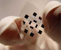 The fabrication of electronic devices on plastic substrates has attracted considerable recent attention owing to the proliferation of handheld, portable consumer electronics. Plastic substrates possess many attractive properties including biocompatibility, flexibility, light weight, shock resistance, softness and transparency. Achieving high performance electronics or sensors on plastic substrates is difficult, because plastics melt at temperatures above 120 degrees C. Central to continued advances in high-performance plastic electronics is the development of robust methods for overcoming this temperature restriction. Unfortunately, high quality semiconductors (such as silicon) require high growth temperatures, so their application to flexible plastics is prohibited. A group of researchers at the California Institute of Technology now showed that highly ordered films of silicon nanowires can be literally glued onto pieces of plastic to make flexible sensors with state-of-the-art sensitivity to a range of toxic chemicals. These nanowires are crystalline wires made out of doped silicon - the mainstay of the computer industry. By etching nanowires into a wafer of silicon, and then peeling them off and transferring them to plastic, they developed a general, parallel, and scalable strategy for achieving high performance electronics on low cost plastic substrates.
Apr 23rd, 2007
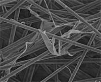
 Tremendous progress has been made over the past few years to control the aspects of fabricating simple nanostructures such as wires, tubes, spheres, cubes etc. However, in order to build functional nanodevices, for instance for nanoelectronics or nanobiotechnology, much more complex nanoarchitectures are needed. Initially, the most common, mostly top-down, fabrication methods used for this purpose have been based on nanolithographic techniques. Unfortunately, these methods are burdened with throughput restrictions and high cost and will be of limited use for commercial mass production of nanostructures. To overcome the limitations of nanolithography, a lot of attention has been focused on self-organized bottom-up approaches, which bear good prospects for large-scale fabrication of nanostructures with controlled morphology and dimensionality, and controlled synthesis of arrays. However, the fabrication of complex nanoarchitectures requires sophisticated transfer techniques, which are far from routine, time consuming, and with low reproducibility. To add to the arsenal of scaleable bottom-up fabrication processes, researchers in Germany have developed a method for the batch fabrication of 3D-nanostructures with tunable surface properties. Resembling suspended nanowire webs, these structures have a high potential for catalytic, sensing, or fluidic applications where a high surface to volume ratio is required.
Mar 29th, 2007
 People involved in designing and developing biosensing applications have high hopes that their field can benefit from nanotechnology. The term biosensing relates to systems that include electronic, photonic, biologic, chemical and mechanical means for producing signals that can be used for the identification, monitoring or control of biological phenomena. The resulting biosensors are devices that employ biological components such as proteins to provide selectivity and/or amplification for the detection of biochemical materials for use in medical diagnostics, environmental analysis or chemical and biological warfare agent detection. Applying nanotechnology to biosensors opens up novel detection possibilities thanks to the nano-physical properties of certain materials. A lot of research worldwide is devoted to developing nanobiosensors. A group in Switzerland, for example, is working on the development of two different kinds of label-free biosensors. One is a nanowire array, the other an optical biosensor based on localized surface plasmon resonance.
Mar 28th, 2007
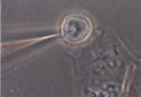 Biosensors, which incorporate biological probes coupled to a transducer, have been developed during the last two decades for environmental, industrial, and biomedical diagnostics. The application of nanotechnology to biosensor design and fabrication promises to revolutionize diagnostics and therapy at the molecular and cellular level. The convergence of nanotechnology, biology, and photonics opens the possibility of detecting and manipulating atoms and molecules using a new class of fiberoptic biosensing and imaging nanodevices. These nanoprobes and nanosensors have the potential for a wide variety of medical uses at the cellular level. The potential for monitoring in vivo biological processes within single living cells, e.g. the capacity to sense individual chemical species in specific locations within a cell, will greatly improve our understanding of cellular function, thereby revolutionizing cell biology. Existing nanoprobes have already demonstrated the capability of performing biologically relevant measurements inside single living cells.
Mar 23rd, 2007
 The challenges in transportation security, most notably air transport, evolve around detecting explosives before they reach their target, i.e. get on a plane for instance. The two technology-based methods of explosive detection are either nuclear-based (probing the screened object with highly penetrating radiation) or rely on trace detection. Trace detection techniques use separation and detection technologies, such as mass spectrometry, gas chromatography, chemical luminescence, or ion mobility spectrometry, to measure the chemical properties of vapor or particulate matter collected from passengers or luggage. All these methods require bulky and expensive equipment, costing hundreds of thousands of dollars apiece. This results in a situation where the effort and technology involved in the detection of explosives are orders of magnitude more expensive than the effort and costs incurred by terrorists in their deployment. Today, the cheapest, very reliable, and most mobile form of explosive detection is decidedly low-tech - dogs. The olfactory ability of dogs is sensitive enough to detect trace amounts of many compounds, which makes them very effective in screening objects. A dog can search an entire airport in a couple of hours. Using a chemical analysis machine would mean wiping down nearly every surface in the airport with a sterile cotton pad, then sticking those pads, one by one, into a computer for analysis. Given the recent advances of nanotechnology, researchers are now trying to develop the next generation of explosives sensors that are accurate, fast, portable and inexpensive - and don't need to be fed.
Mar 13th, 2007
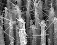
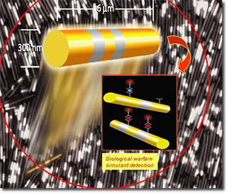 In an effort to detect biological threats quickly and accurately, a number of detection technologies have been developed. This rapid growth and development in biodetection technology has largely been driven by the emergence of new and deadly infectious diseases and the realization of biological warfare as new means of terrorism. To address the need for portable, multiplex biodetection systems a number of immunoassays have been developed. An immunoassay is a biochemical test that measures the level of a substance in a biological liquid. The assay takes advantage of the specific binding of an antigen to its antibody, the proteins that the body produces to directly attack, or direct the immune system to attack, cells that have been infected by viruses, bacteria and other intruders. Physical, chemical and optical properties that can be tuned to detect a particular bioagent are key to microbead-based immunoassay sensing systems. A unique spectral signature or fingerprint can be tied to each type of bead. Beads can be joined with antibodies to specific biowarfare agents. A recently developed novel biosensing platform uses engineered nanowires as an alternative substrate for immunoassays. Nanowires built from sub-micrometer layers of different metals, including gold, silver and nickel, are able to act as "barcodes" for detecting a variety of pathogens, such as anthrax, smallpox, ricin and botulinum toxin. The approach could simultaneously identify multiple pathogens via their unique fluorescent characteristics.
Mar 8th, 2007
 Subscribe to our Nanotechnology Spotlight feed